
High rectification and gate-tunable photoresponse in 1D-2D lateral van der waals heterojunctions
-
GRAPHICAL ABSTRACT
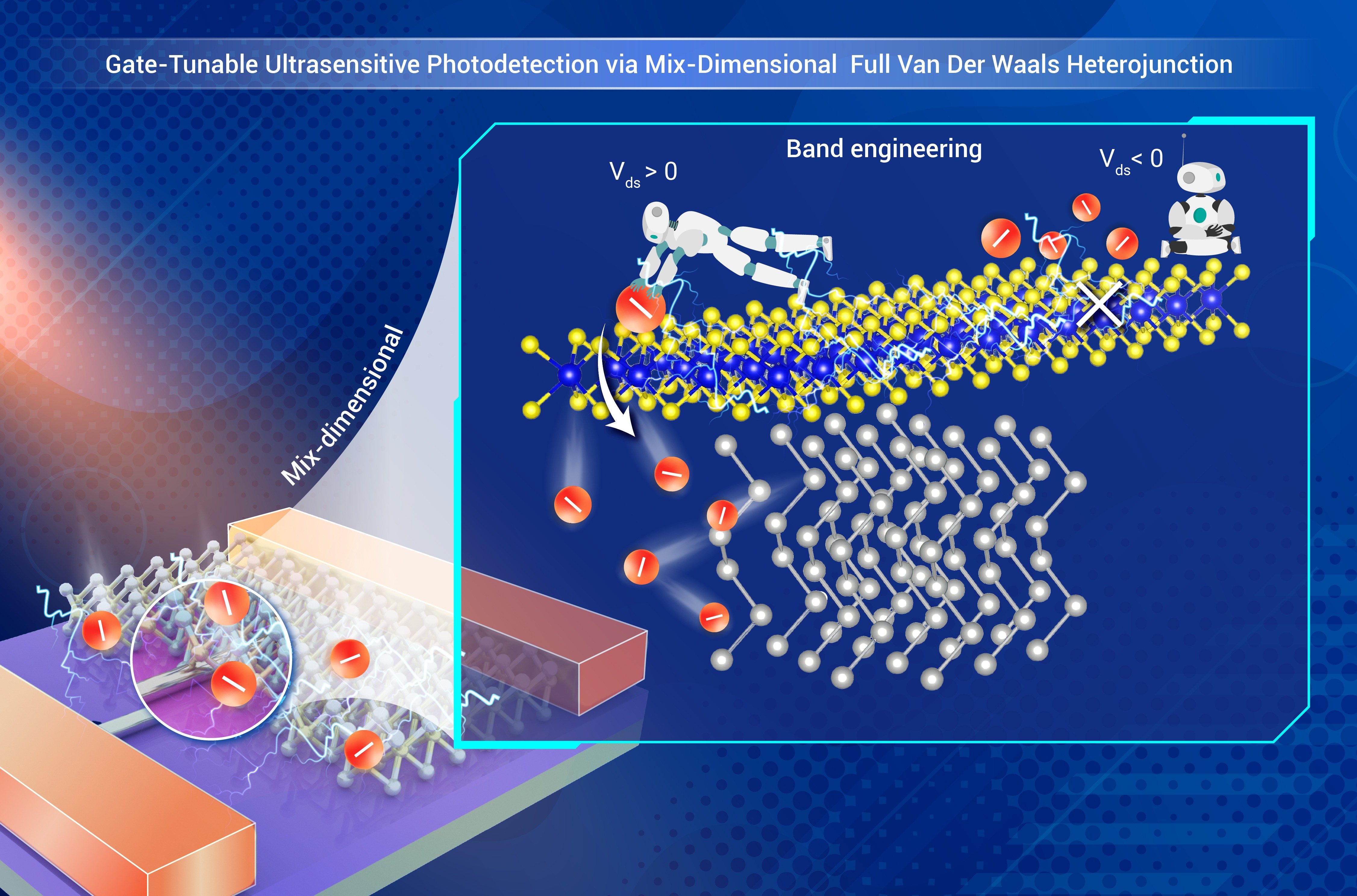
 DownLoad:
Full size image
DownLoad:
Full size image
-
PUBLIC SUMMARY
-
Fully van der Waals-integrated (vdWs) gate-tunable photodiode based on 1D Te–2D WS2 heterojunction.
Achieves both a high rectification ratio and on/off ratio simultaneously, with ultra-low dark current.
High detectivity enables ultra-weak light detection, along with fast response time and excellent linearity.
New insights into vdWs optoelectronics through band engineering, dimensional control, and interface design.
-
-
ABSTRACT
The self-passivating surfaces and reduced tunneling leakage current enable the creation of ideal Schottky contacts in van der Waals (vdW) semiconductor heterojunctions. However, simultaneously achieving high rectification ratios, low reverse leakage currents, and rapid photoresponse remains challenging. Here, we present a one-dimensional (1D)/two-dimensional (2D) mixed-dimensional heterostructure photodiode to address these challenges. The significant valence band offset and minimal electron affinity difference in this structure ensure high rectification ratios and efficient charge collection. Additionally, the dimensional disparity between the 1D and 2D materials, characterized by a smaller contact area and significant thickness difference, results in low reverse leakage current and a high current on-off ratio. Moreover, it enables gate-tunable band structure transitions. Our device exhibits an exceptional rectifying ratio of 4.7 × 10⁷ and a high on-off ratio of 5 × 10⁷ (Vds = 2 V and, Vg = 30 V) at room temperature. Under a gate voltage of 20 V, the photodiode achieves a specific detectivity (D*) of 4.9 × 10¹⁴ Jones, a rapid response time of 14 μs, and an extended operational wavelength approaching to1550 nm. The strategic combination of mixed-dimensional design and band engineering yields a 1D-2D p-n heterojunction photodiode with remarkable sensitivity, repeatability, and fast response, underscoring the potential of vdW semiconductors for advanced optoelectronic applications.-
Keywords:
- van der Waals heterostructure /
- photodiode /
- rectification ratio /
- gate-tunable /
- Te nanowire /
- WS2
-

-
REFERENCES
[1] Michel J., Liu J. and Kimerling L. C. (2010). High-performance Ge-on-Si photodetectors. Nat. Photonics 4:527−534. DOI:10.1038/nphoton.2010.157 [2] Lee J., Georgitzikis E., Hermans Y., et al. (2023). Thin-film image sensors with a pinned photodiode structure. Nat. Electron. 6:590−598. DOI:10.1038/s41928-023-01016-9 [3] Lischke S., Peczek A., Morgan J. S., et al. (2021). Ultra-fast germanium photodiode with 3-dB bandwidth of 265 GHz. Nat. Photonics 15:925−931. DOI:10.1038/s41566-021-00893-w [4] Wang P., Lan Y., Huan C., et al. (2023). Recent progress on performance-enhancing strategies in flexible photodetectors: From structural engineering to flexible integration. Mater. Sci. Eng. R Rep. 156 :100759. DOI: 10.1016/j.mser.2023.100759 [5] Geim A. K. and Grigorieva I. V. (2013). Van der Waals heterostructures. Nature 499:419−425. DOI:10.1038/nature12385 [6] Jariwala D., Marks T. J. and Hersam M. C. (2017). Mixed-dimensional van der Waals heterostructures. Nat. Mater. 16:170−181. DOI:10.1038/nmat4703 [7] Zhuang R., Cai S., Mei Z., et al. (2023). Solution-grown BiI/BiI3 van der Waals heterostructures for sensitive X-ray detection. Nat. Commun. 14:1621. DOI:10.1038/s41467-023-37297-z [8] Liu Y., Guo J., Zhu E., et al. (2018). Approaching the Schottky–Mott limit in van der Waals metal–semiconductor junctions. Nature 557:696−700. DOI:10.1038/s41586-018-0129-8 [9] Mu H., Zhuang R., Cui N., et al. (2023). Alternating BiI3–BiI van der Waals photodetector with low dark current and high-performance photodetection. ACS Nano 17:21317−21327. DOI:10.1021/acsnano.3c05849 [10] Wang Y., Mei L., Li Y., et al. (2024). Integration of two-dimensional materials based photodetectors for on-chip applications. Phys. Rep. 1081 :1-46. DOI: https://doi.org/10.1016/j.physrep.2024.06.001 [11] Zhang X., Liu B., Gao L., et al. (2021). Near-ideal van der Waals rectifiers based on all-two-dimensional Schottky junctions. Nat. Commun. 12:1522. DOI:10.1038/s41467-021-21861-6 [12] Wang G., Sun Y., Yang Z., et al. (2024). Near-ideal Schottky junction photodetectors based on semimetal-semiconductor van der Waals heterostructures. Adv. Funct. Mater. 34 :2316267. DOI: 10.1002/adfm.202316267. [13] LaGasse S. W., Dhakras P., Watanabe K., et al. (2019). Gate-tunable graphene–WSe2 heterojunctions at the Schottky–Mott limit. Adv. Mater. 31 :1901392. DOI: 10.1002/adma.201901392 [14] Huo N. and Konstantatos G. (2017). Ultrasensitive all-2D MoS2 phototransistors enabled by an out-of-plane MoS2 PN homojunction. Nat. Commun. 8:572. DOI:10.1038/s41467-017-00722-1 [15] Buscema M., Groenendijk D. J., Steele G. A., et al. (2014). Photovoltaic effect in few-layer black phosphorus PN junctions defined by local electrostatic gating. Nat. Commun. 5:4651. DOI:10.1038/ncomms5651 [16] Huang M., Li S., Zhang Z., et al. (2017). Multifunctional high-performance van der Waals heterostructures. Nat. Nanotechnol. 12:1148−1154. DOI:10.1038/nnano.2017.208 [17] Yu W. J., Li Z., Zhou H., et al. (2013). Vertically stacked multi-heterostructures of layered materials for logic transistors and complementary inverters. Nat. Mater. 12:246−252. DOI:10.1038/nmat3518 [18] Kang J., Jariwala D., Ryder C. R., et al. (2016). Probing out-of-plane charge transport in black phosphorus with graphene-contacted vertical field-effect transistors. Nano Lett. 16:2580−2585. DOI:10.1021/acs.nanolett.6b00144 [19] Wu F., Li Q., Wang P., et al. (2019). High efficiency and fast van der Waals hetero-photodiodes with a unilateral depletion region. Nat. Commun. 10:4663. DOI:10.1038/s41467-019-12707-3 [20] Cheng R., Wang F., Yin L., et al. (2018). High-performance, multifunctional devices based on asymmetric van der Waals heterostructures. Nat. Electron. 1:356−361. DOI:10.1038/s41928-018-0086-0 [21] Tan C., Yin S., Chen J., et al. (2021). Broken-gap PtS2/WSe2 van der Waals heterojunction with ultrahigh reverse rectification and fast photoresponse. ACS Nano 15:8328−8337. DOI:10.1021/acsnano.0c09593 [22] Wang Y., Qiu G., Wang R., et al. (2018). Field-effect transistors made from solution-grown two-dimensional tellurene. Nat. Electron. 1:228−236. DOI:10.1038/s41928-018-0058-4 [23] Qin J.-K., Liao P.-Y., Si M., et al. (2020). Raman response and transport properties of tellurium atomic chains encapsulated in nanotubes. Nat. Electron. 3:141−147. DOI:10.1038/s41928-020-0365-4 [24] Wu W., Qiu G., Wang Y., et al. (2018). Tellurene: its physical properties, scalable nanomanufacturing, and device applications. Chem. Soc. Rev. 47:7203−7212. DOI:10.1039/C8CS00598B [25] Yu J., Mu H., Wang P., et al. (2024). Anisotropic van der Waals tellurene-based multifunctional, polarization-sensitive, in-line optical device. ACS Nano 18:19099−19109. DOI:10.1021/acsnano.4c03973 [26] Zhao W., Ghorannevis Z., Chu L., et al. (2013). Evolution of electronic structure in atomically thin sheets of WS2 and WSe2. ACS Nano 7:791−797. DOI:10.1021/nn305275h [27] Hong X., Kim J., Shi S.-F., et al. (2014). Ultrafast charge transfer in atomically thin MoS2/WS2 heterostructures. Nat. Nanotechnol. 9:682−686. DOI:10.1038/nnano.2014.167 [28] Seib D. H. and Aukerman L. W. (1973). Photodetectors for the 0.1 to 1.0 μm spectral region. Marton L. and Marton C. (Eds). Adv. Electron. Electron Phys. (Academic Press) 34 , pp 95-221. [29] Went C. M., Wong J., Jahelka P. R., et al. (2019). A new metal transfer process for van der Waals contacts to vertical Schottky-junction transition metal dichalcogenide photovoltaics. Sci. Adv. 5:eaax6061. DOI:10.1126/sciadv.aax6061 [30] Kresse G. and Furthmüller J. (1996). Efficient iterative schemes for ab initio total-energy calculations using a plane-wave basis set. Phys. Rev. B 54:11169−11186. DOI:10.1103/PhysRevB.54.11169 [31] Kresse G. and Furthmüller J. (1996). Efficiency of ab-initio total energy calculations for metals and semiconductors using a plane-wave basis set. Comput. Mater. Sci. 6 :15-50. DOI: 10.1016/0927-0256(96)00008-0 [32] Perdew J. P., Burke K. and Ernzerhof M. (1996). Generalized gradient approximation made simple. Phys. Rev. Lett. 77:3865−3868. DOI:10.1103/PhysRevLett.77.3865 [33] Wang F., Liu Z., Zhang T., et al. (2022). Fully depleted self-aligned heterosandwiched van der Waals photodetectors. Adv. Mater. 34 :2203283. DOI: 10.1002/adma.202203283 [34] Garrity O., Rodriguez A., Mueller N. S., et al. (2022). Probing the local dielectric function of WS2 on an Au substrate by near field optical microscopy operating in the visible spectral range. Appl. Surf. Sci. 574 :151672. DOI: 10.1016/j.apsusc.2021.151672 [35] Sharma T., Thakur R. and Sharma R. (2021). Structural, electronic and dielectric properties of tellurium 1-D nanostructures : a DFT study. Appl. Phys. A 128:41. DOI:10.1007/s00339-021-05183-4 [36] Luo L.-B., Liang F.-X., Huang X.-L., et al. (2012). Tailoring the electrical properties of tellurium nanowires via surface charge transfer doping. J. Nanopart. Res. 14:967. DOI:10.1007/s11051-012-0967-5 [37] Rogalski A. (2022). Detectivities of WS2/HfS2 heterojunctions. Nat. Nanotechnol. 17:217−219. DOI:10.1038/s41565-022-01076-6 [38] Wu X., Kalliopuska J. and Eränen S., et al. (2012). Recent advances in processing and characterization of edgeless detectors. J. Instrum 7:C02001. DOI:10.1088/1748-0221/7/02/C02001 [39] Ren D., Meng X., Rong Z., et al. (2018). Uncooled photodetector at short-wavelength infrared using InAs nanowire photoabsorbers on InP with p–n heterojunctions. Nano Lett. 18:7901−7908. DOI:10.1021/acs.nanolett.8b03775 [40] Shockley W. (1949). The theory of p-n junctions in semiconductors and p-n junction transistors. Bell Syst. Tech. J 28:435−489. DOI:10.1002/j.1538-7305.1949.tb03645.x [41] Sah C. t., Noyce R. N. and Shockley W. (1957). Carrier generation and recombination in P-N Junctions and P-N junction characteristics. Proc. IRE 45:1228−1243. DOI:10.1109/JRPROC.1957.278528 [42] Chen Y., Wang Y., Wang Z., et al. (2021). Unipolar barrier photodetectors based on van der Waals heterostructures. Nat. Electron. 4:357−363. DOI:10.1038/s41928-021-00586-w [43] Williams K. J. and Esman R. D. (1999). Design considerations for high-current photodetectors. J. Lightwave Technol. 17:1443−1454. DOI:10.1109/50.779167 [44] Wang W., Wang W., Meng Y., et al. (2022). Mixed-dimensional anti-ambipolar phototransistors based on 1D GaAsSb/2D MoS2 heterojunctions. ACS Nano 16:1036−11048. DOI:10.1021/acsnano.2c03673 [45] You J., Jin Z., Li Y., et al. (2024). Epitaxial growth of 1D Te/2D MoSe2 mixed-dimensional heterostructures for high-efficient self-powered photodetector. Adv. Funct. Mater. 34 :2311134. DOI: 10.1002/adfm.202311134. [46] Tao J.-J., Jiang J., Zhao S.-N., et al. (2021). Fabrication of 1D Te/2D ReS2 mixed-dimensional van der Waals p-n heterojunction for high-performance phototransistor. ACS Nano 15:3241−3250. DOI:10.1021/acsnano.0c09912 [47] Wu F., Xia H., Sun H., et al. (2019). AsP/InSe van der Waals tunneling heterojunctions with ultrahigh reverse rectification ratio and high photosensitivity. Adv. Funct. Mater. 29 :1900314. DOI: 10.1002/adfm.201900314 -
ABOUT THIS ARTICLE
Cite this article:
Wang P., Mu H., Yun T., et al. (2025). High rectification and gate-tunable photoresponse in 1D-2D lateral van der waals heterojunctions. The Innovation Materials 3:100113. https://doi.org/10.59717/j.xinn-mater.2024.100113
Welcome!
To request copyright permission to republish or share portions of our works, please visit Copyright Clearance Center's (CCC) Marketplace website at marketplace.copyright.com.
Article Metrics
Relative Articles
Cited by
Export File
Citation
Wang P., Mu H., Yun T., et al. (2025). High rectification and gate-tunable photoresponse in 1D-2D lateral van der waals heterojunctions. The Innovation Materials 3:100113. https://doi.org/10.59717/j.xinn-mater.2024.100113

Format
Content


-
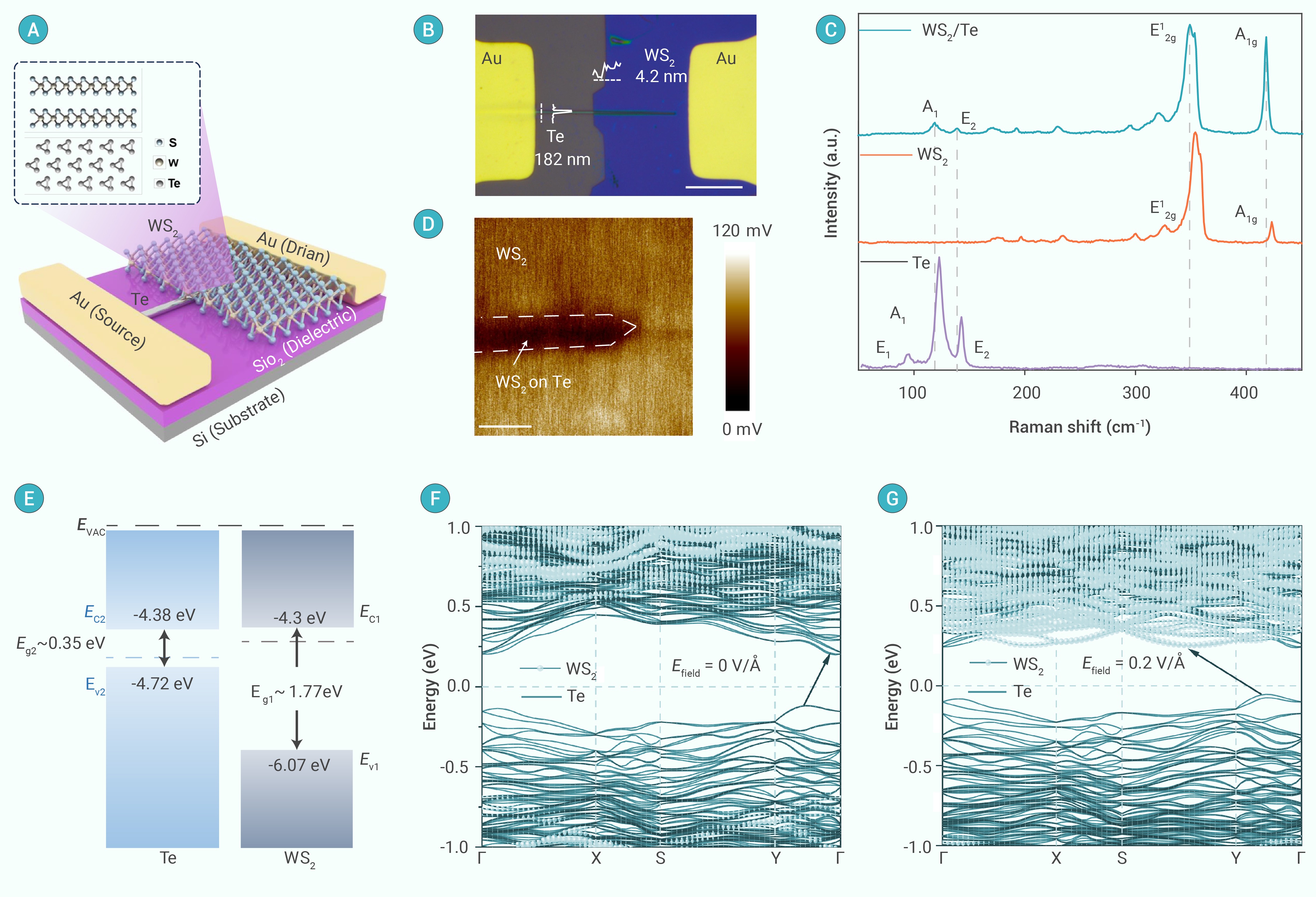
Figure 1.
Schematic and characterization of the vdWs photodiode
-
Figure 2.
Electrical transport properties of the Te/WS2 heterojunction device
-
Figure 3.
Optoelectronic response of the Te/WS2 photodiode device without gate modulation
-
Figure 4.
Gate-modulated photoresponse characteristics of Te/WS2 heterojunction photodiodes
-
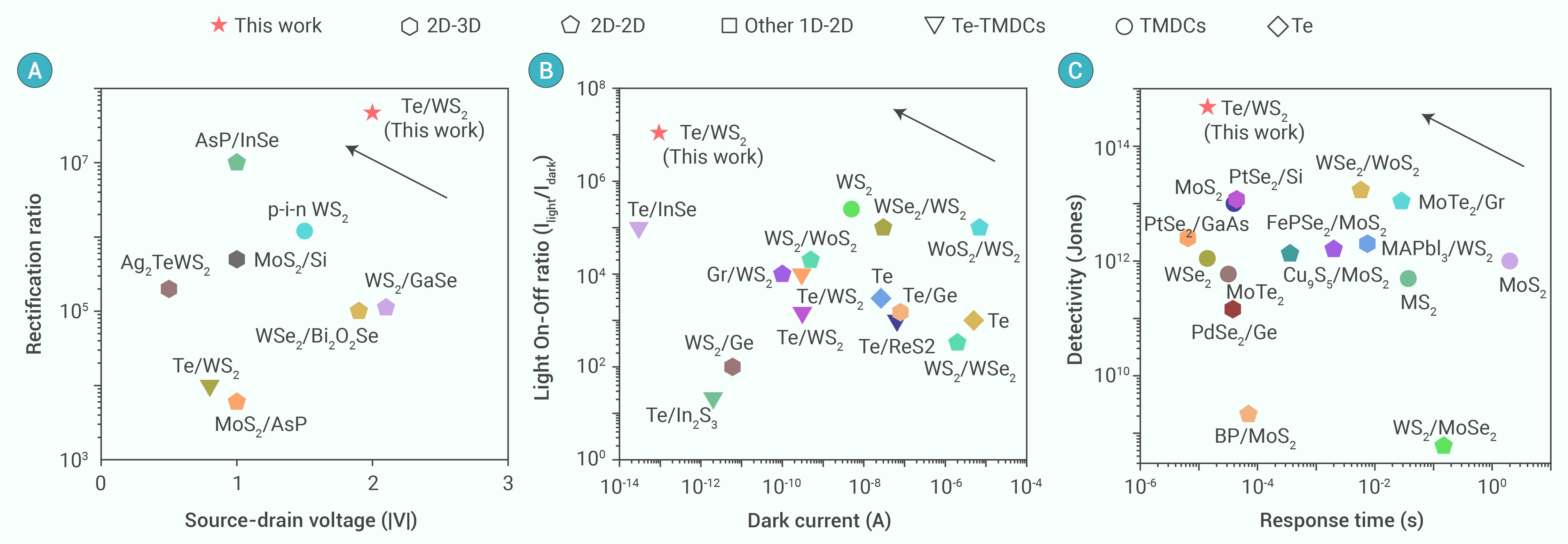
Figure 5.
Benchmarking the performance of the Te/WS2 heterojunction photodiode against other 2D material-based photodetectors
