
Revealing the atomic-scale structures of dislocations in calcium fluoride single crystal
-
GRAPHICAL ABSTRACT
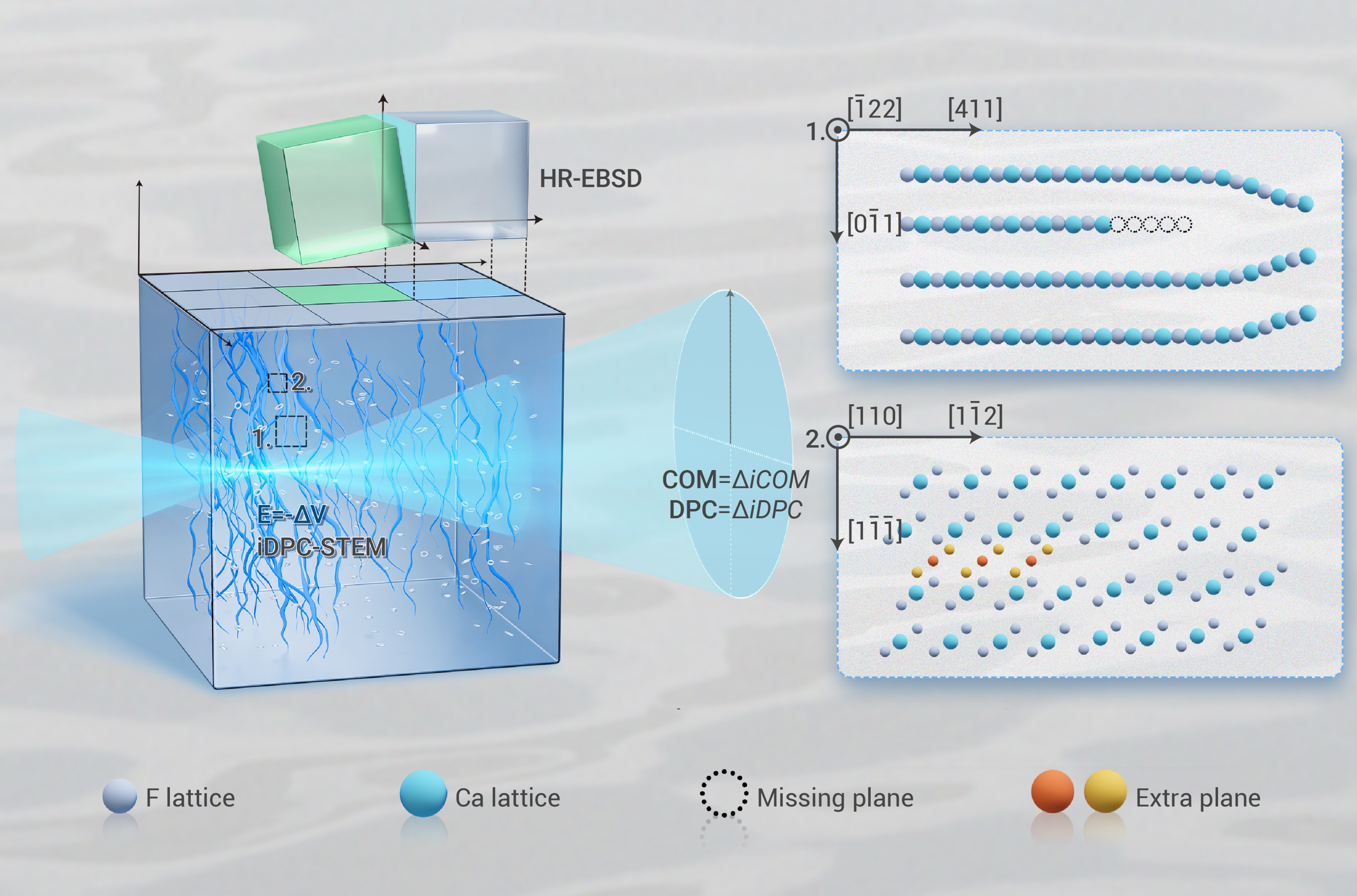
 DownLoad:
Full size image
DownLoad:
Full size image
-
PUBLIC SUMMARY
-
The atomic structure of dislocations were identified by utilizing a combination of characterization methods.
The underlying mechanism responsible for dislocation formation is revealed.
Strategies for suppressing the formation of dislocations are proposed.
-
-
ABSTRACT
Dislocations are ubiquitous in crystalline solids and play a critical role in both material properties and device performance. Due to the numerous variables influencing crystal growth, such as temperature, pressure, and impurity levels, the synthesis of high-quality crystals with minimal defects remains a challenging and enduring goal in crystal research. Calcium fluoride (CaF2) which is widely used in optical devices typically contains dislocations on the order of 10-5 cm-2. The sensitivity of the weak CaF2 lattice to electron beams makes at atomic-level imaging using traditional scanning transmission electron microscopy difficult. Here, we utilize a combination of characterization methods to analyze the microstructure of dislocations in CaF2, and the existence of both stored statistical dislocations (SSDs) and geometrically necessary dislocations (GNDs) are identified. SSDs mainly consist of perfect dislocations with a small amount of Frank partial dislocations, while GNDs are predominantly composed of Frank partial dislocations and stacking faults. Based on the calculated formation energies of dislocations and fluorite vacancies, the formation mechanisms of SSDs and GNDs are proposed. The findings in the present study deepen our understanding of the dislocations in CaF2 and offer insights into strategies to further reduce the defect concentration in CaF2 crystals. -

-
REFERENCES
[1] Dominguez J. E., Fu L. and Pan X. Q. (2002). Effect of crystal defects on the electrical properties in epitaxial tin dioxide thin films. Appl. Phys. Lett. 81:5168. DOI:10.1063/1.1530745 [2] Hwang J. Y., Kim J., Kim H. S., et al. (2018). Effect of dislocation arrays at grain boundaries on electronic transport properties of bismuth antimony telluride: Unified strategy for high thermoelectric performance. Adv. Energy Mater. 8:1800065. DOI:10.1002/aenm.201800065 [3] Armstrong M. D., Lan K. W., Guo Y., et al. (2021). Dislocation-mediated conductivity in oxides: Progress, challenges, and opportunities. ACS nano 15:9211. DOI:10.1021/acsnano.1c01557 [4] Pratt P. L., Roy C. and Evans A. G. (1966). The role of grain boundaries in the plastic deformation of calcium fluoride. Conference: The role of grain boundaries and surfaces in ceramics. DOI:10.1007/978-1-4899-6311-6_14. [5] Jena D. and Mishra U. K. (2002). Effect of scattering by strain fields surrounding edge dislocations on electron transport in two-dimensional electron gases. Appl. Phys. Lett. 80:64. DOI:10.1063/1.1429758 [6] Zhou S., Zhao X., Du P., et al. (2022). Application of patterned sapphire substrate for III-nitride light-emitting diodes. Nanoscale. 14:4887. DOI:10.1039/D1NR08221C [7] Moriya K. (1991). Light scattering from defects in crystals: scattering by dislocations. Philos. Mag. B 64:425. DOI:10.1080/13642819108215267 [8] Tanikawa T., Ohnishi K., Kanoh M., et al. (2018). Three-dimensional imaging of threading dislocations in GaN crystals using two-photon excitation photoluminescence. Appl. Phys. Express. 11:031004. DOI:10.7567/APEX.11.031004 [9] Ben J., Sun X., Jia Y., et al. (2019). Influence of dislocations on the refractive index of AlN by nanoscale strain field. Nanoscale Res. Lett. 14:1. DOI:10.1186/s11671-019-3018-7 [10] Hoshikawa K., Huang X., Taishi T., et al. (1999). Dislocation-Free Czochralski Silicon Crystal Growth without the Dislocation-Elimination-Necking Process. J. Appl. Phys. (Japan). 38:L1369. DOI:10.1143/JJAP.38.L1369 [11] Yang G., Liu X., Xu L., et al. (2022). Dislocations in 4H silicon carbide single crystals. J. Synth. Cryst. 51:1673. DOI:10.4028/www.scientifc.net/MSF.858.393 [12] Manning I., Matsuda Y., Chung G., et al. (2020). Progress in bulk 4H SiC crystal growth for 150 mm wafer production. Conference: MSF. 1004:37. DOI:10.4028/www.scientific.net/MSF.1004.37 [13] Wang G., Zhang M., Zuo H., et al. (2007). Dislocation analysis for large-sized sapphire single crystal grown by SAPMAC method. Chinese. J. Struct. Chem. 26:1332. DOI:10.14102/j.cnki.0254-5861.2007.11.023 [14] Muzy J., Fivel M., Labor S., et al. (2023). Influence of growth process and crystal defects on sapphire brittleness. J. Cryst. Growth. 618:127327. DOI:10.1016/j.jcrysgro.2023.127327 [15] Motzer C. and Reichling M. (2009). High resolution study of etch figures on CaF2 (111). J. Appl. Phys. 105:064309. DOI:10.1063/1.3078774 [16] Abrahams M. S. and Herkart P. G. (1965). Effects of growth parameters on dislocations in CaF2. J. Appl. Phys. 36:274. DOI:10.1063/1.1713890 [17] Bioud Y. A., Boucherif A., Myronov M., et al. (2019). Uprooting defects to enable high-performance III–V optoelectronic devices on silicon. Nat. Commun. 10:4322. DOI:10.1038/s41467-019-12353-9 [18] Taylor P. J., Jesser W. A., Benson J. D., et al. (2001). Optoelectronic device performance on reduced threading dislocation density GaAs/Si. J. Appl. Phys. 89:4365. DOI:10.1063/1.1347000 [19] Cherns D. (2000). The structure and optoelectronic properties of dislocations in GaN. J. Phys: Condens. Matter. 12:10205. DOI:10.1088/0953-8984/12/49/320 [20] Fahey P. M., Mader S. R., Stiffler S. R., et al. (1992). Stress-induced dislocations in silicon integrated circuits. IBM J. Res. Dev. 36:158. DOI:10.1147/rd.362.0158 [21] Kittler M. and Reiche M. (2009). Dislocations as active components in novel silicon devices. Adv. Eng. Mater. 11:249. DOI:10.1002/adem.200800283 [22] Evans A. G. and Pratt P. L. (1969). Dislocations in the fluorite structure. Philos. Mag. 20:1213. DOI:10.1080/14786436908228207 [23] Keig G. A. and Coble R. L. (1968). Mobility of edge dislocations in single-crystal calcium fluoride. J. Appl. Phys. 39:6090. DOI:10.1063/1.1656121 [24] Katz R. N. and Coble R. L. (1974). Effect of neodymium on dislocation velocity in CaF2. J. Appl. Phys. 45:2382. DOI:10.1063/1.1663601 [25] Sadrabadi P., Eisenlohr P., Wehrhan G., et al. (2009). Evolution of dislocation structure and deformation resistance in creep exemplified on single crystals of CaF2. Mater. Sci. Eng. A. 510:46. DOI:10.1016/j.msea.2008.04.086 [26] Motzer C. and Reichling M. (2010). Morphological classification and quantitative analysis of etch pits. J. Appl. Phys. 108:113523. DOI:10.1063/1.3510535 [27] Kuhlmann-Wilsdorf D. (1989). Theory of plastic deformation:-properties of low energy dislocation structures. Mater. Sci. Eng. A 113:1. DOI:10.1016/0921-5093(89)90290-6 [28] Tao N. R., Wang Z. B., Tong W. P., et al. (2002). An investigation of surface nanocrystallization mechanism in Fe induced by surface mechanical attrition treatment. Acta Mater. 50:4603. DOI:10.1016/S1359-6454(02)00310-5 [29] Landau P., Shneck R., Makov G., et al. (2009). Evolution of dislocation patterns in fcc metals. Conference: IOP Conf. Ser. Mater. Sci. Eng. 3:012004. DOI:10.1088/1757-899X/3/1/012004 [30] Wu X., Tao, N., Hong Y., et al. (2002). Microstructure and evolution of mechanically-induced ultrafine grain in surface layer of AL-alloy subjected to USSP. Acta Mater. 50:2075. DOI:10.1016/S1359-6454(02)00051-4 [31] Tang C., Wan W., Huang L., et al. (2022). On the formation and multiplicity of Si [001] small angle symmetric Tilt grain boundaries: Atomistic simulation of directional growth. Cryst. Growth Des. 22:7491. DOI:10.1021/acs.cgd.2c01046 [32] Rolland P., Dicks K. and Ravel-Chapuis R. (2002). EBSD spatial resolution in the SEM when analyzing small grains or deformed material. Microsc. Microanal. 8:670. DOI:10.1017/S1431927602106350 [33] Lehto P. (2021). Adaptive domain misorientation approach for the EBSD measurement of deformation induced dislocation sub-structures. Ultramicroscopy. 222:113203. DOI:10.1016/j.ultramic.2021.113203 [34] Sadrabadi P., Durst K., Göken M., et al. (2009). Quantification of dislocation structures at high resolution by atomic force microscopy of dislocation etch pits. Philos. Mag. Lett. 89:391. DOI:10.1080/09500830902984554 [35] Wang Y., Brodusch N., Gauvin R., et al. (2022). Line-rotated remapping for high-resolution electron backscatter diffraction. Ultramicroscopy. 242:113623. DOI:10.1016/j.ultramic.2022.113623 [36] Murr L. E. (1974). Transmission electron microscope study of crystal defects in natural fluorite. Phys. Status. Solidi. A 22:239. DOI:10.1002/pssa.2210220128 [37] Chadderton L. T., Johnson E. and Wohlenberg T. (1976). Observations of a regular void array in natural fluorite irradiated with 100 keV electrons. Phys. Scr. 13:127. DOI:10.1088/0031-8949/13/2/012 [38] Karlušić M., Ghica C., Negrea R. F., et al. (2017). On the threshold for ion track formation in CaF2. New J. Phys. 19:023023. DOI:10.1088/1367-2630/aa5914 [39] Lazić I. and Bosch, E. G. (2017). Analytical review of direct STEM imaging techniques for thin samples. Adv. Imaging Electron Phys. 199:75. DOI:10.1016/bs.aiep.2017.01.006 [40] Bosch E. G. and Lazić I. (2015). Analysis of HR-STEM theory for thin specimen. Ultramicroscopy. 156:59. DOI:10.1016/j.ultramic.2015.02.004 [41] Krivanek O. L., Chisholm M. F., Nicolosi, V. et al. (2010). Atom-by-atom structural and chemical analysis by annular dark-field electron microscopy. Nature. 464:571. DOI:10.1038/nature08879 [42] Yücelen E. Lazić I. and Bosch E. G. T. (2018). Phase contrast scanning transmission electron microscopy imaging of light and heavy atoms at the limit of contrast and resolution. Sci. Rep. 8:2676. DOI:10.1038/s41598-018-20377-2 [43] Ma Y., Cai D., Li Y., et al. (2016). The influence of straight pore blockage on the selectivity of methanol to aromatics in nanosized Zn/ZSM-5: An atomic Cs-corrected STEM analysis study. RSC Adv. 6:74797. DOI:10.1039/C6RA19073A [44] Shen B., Chen X., Shen K., et al. (2020). Imaging the node-linker coordination in the bulk and local structures of metal-organic frameworks. Nat. Commun. 11:2692. DOI:10.1038/s41467-020-16531-y [45] Shen B., Wang H., Xiong H., et al. (2022). Atomic imaging of zeolite-confined single molecules by electron microscopy. Nature. 607:703. DOI:10.1038/s41586-022-04876-x [46] Bhattacharjee S., Chen C. and Ahn W. S. (2014). Chromium terephthalate metal–organic framework MIL-101: synthesis, functionalization, and applications for adsorption and catalysis. RSC Adv. 4:52500. DOI:10.1039/C4RA11259H [47] Ma M., Zhang X., Chen X., et al. (2023). In situ imaging of the atomic phase transition dynamics in metal halide perovskites. Nat. Commun. 14:7142. DOI:10.1038/s41467-023-42999-5 [48] Liu B., Chen X., Huang N., et al. (2023). Imaging the dynamic influence of functional groups on metal-organic frameworks. Nat. Commun. 14:4835. DOI:10.1038/s41467-023-40590-6 [49] Zhang H., Li G., Zhang J., et al. (2023). Three-dimensional inhomogeneity of zeolite structure and composition revealed by electron ptychography. Science. 380:633. DOI:10.1126/science.adg3183 [50] Hohenberg P. and Kohn W. (1964). Inhomogeneous Electron Gas. Phys. Rev. 136:B864. DOI:10.1103/PhysRev.136.B864 [51] Kresse G. and Furthmüller J. (1996). Efficient iterative schemes for ab initio total-energy calculations using a plane-wave basis set. Phys. Rev. B. 54:11169. DOI:10.1103/PhysRevB.54.11169 [52] Kresse G. and Hafner J. (1993). Ab initio molecular dynamics for liquid metals. Phys. Rev. B. 47:558. DOI:10.1103/PhysRevB.47.558 [53] Kresse G. and Hafner J. (1994). Ab initio molecular-dynamics simulation of the liquid-metal--amorphous-semiconductor transition in germanium. Phys. Rev. B 49:14251. DOI:10.1103/PhysRevB.49.14251. [54] Kresse G. and Furthmüller J. (1996). Efficiency of ab-initio total energy calculations for metals and semiconductors using a plane-wave basis set. Comput. Mater. Sci. 6:15. DOI:10.1016/0927-0256(96)00008-0 [55] Blöchl P. E. (1994). Projector augmented-wave method. Phys. Rev. B 50:17953. DOI:10.1103/PhysRevB.50.17953 [56] Perdew J. P., Burke K. and Wang Y. (1996). Generalized gradient approximation for the exchange-correlation hole of a many-electron system. Phys. Rev. B 54:16533. DOI:10.1103/PhysRevB.54.16533 [57] Perdew J. P., Ruzsinszky A., Csonka G. I., et al. (2008). Restoring the Density-Gradient Expansion for Exchange in Solids and Surfaces. Phys. Rev. Lett. 100:136406. DOI:10.1103/PhysRevLett.100.136406 [58] Monkhorst H. J. and Pack J. D. (1976). Special points for Brillouin-zone integrations. Phys. Rev. B. 13:5188. DOI:10.1103/PhysRevB.13.5188 [59] Blumenau A. T., Heggie M. I., Fall C. J., et al. (2002). Dislocations in diamond: Core structures and energies. Phys. Rev. B. 65:205205. DOI:10.1103/PhysRevB.65.205205 [60] Hÿtch M. J., Putaux J. L. and Pénisson J. M. (2003). Measurement of the displacement field of dislocations to 0.03 Å by electron microscopy. Nature. 423:270. DOI:10.1038/nature01638. [61] Pennycook and Stephen J. (2009). Transmission electron microscopy: A textbook for materials science, Second Edition. Willianms D. B. and Carter C. B. (Springer). DOI:10.1017/S1431927609991140. [62] Bishara H., Lee S., Brink T., et al. (2021). Understanding grain boundary electrical resistivity in Cu: the effect of boundary structure. ACS nano. 15:16607. DOI:10.1021/acsnano.1c06367 [63] Recker K. and Leckebusch R. (1971). Zur Züchtung von CaF2-UND CaF2 (U)-einkristallen aus der dampfphase. J. Cryst. Growth. 9:274. DOI:10.1016/0022-0248(71)90242-9 [64] Bollmann W. (1980). Incorporation of O2- and OH- ions in CaF2 crystals by reaction with the surrounding atmosphere. Phys. Status. Solidi. A 57:601. DOI:10.1002/pssa.2210570217 [65] Cockayne B., Robertson D. S. and Straughan B. W. (1964). Calcium fluoride: slip and polygonization during crystal growth. Nature. 203:1376. DOI:10.1038/2031376a0 [66] Zou J., Fauler A., Senchenkov A. S., et al. (2021). Characterization of structural defects in (Cd, Zn) Te crystals grown by the travelling heater method. Crystals 11:1402. DOI:10.3390/cryst11111402 [67] Kishan Rao K. and Sirdeshmukh D. B. (1990). Indentation studies on alkaline earth fluoride crystals at elevated temperatures. Pramana. 34:151. DOI:10.1007/BF02847199 -
ABOUT THIS ARTICLE
Cite this article:
Li S., Wang Y., Zhang B., et al. (2025). Revealing the atomic-scale structures of dislocations in calcium fluoride single crystal. The Innovation Materials 3:100129. https://doi.org/10.59717/j.xinn-mater.2025.100129
Welcome!
To request copyright permission to republish or share portions of our works, please visit Copyright Clearance Center's (CCC) Marketplace website at marketplace.copyright.com.
Article Metrics
Relative Articles
Cited by
Export File
Citation
Li S., Wang Y., Zhang B., et al. (2025). Revealing the atomic-scale structures of dislocations in calcium fluoride single crystal. The Innovation Materials 3:100129. https://doi.org/10.59717/j.xinn-mater.2025.100129

Format
Content

-
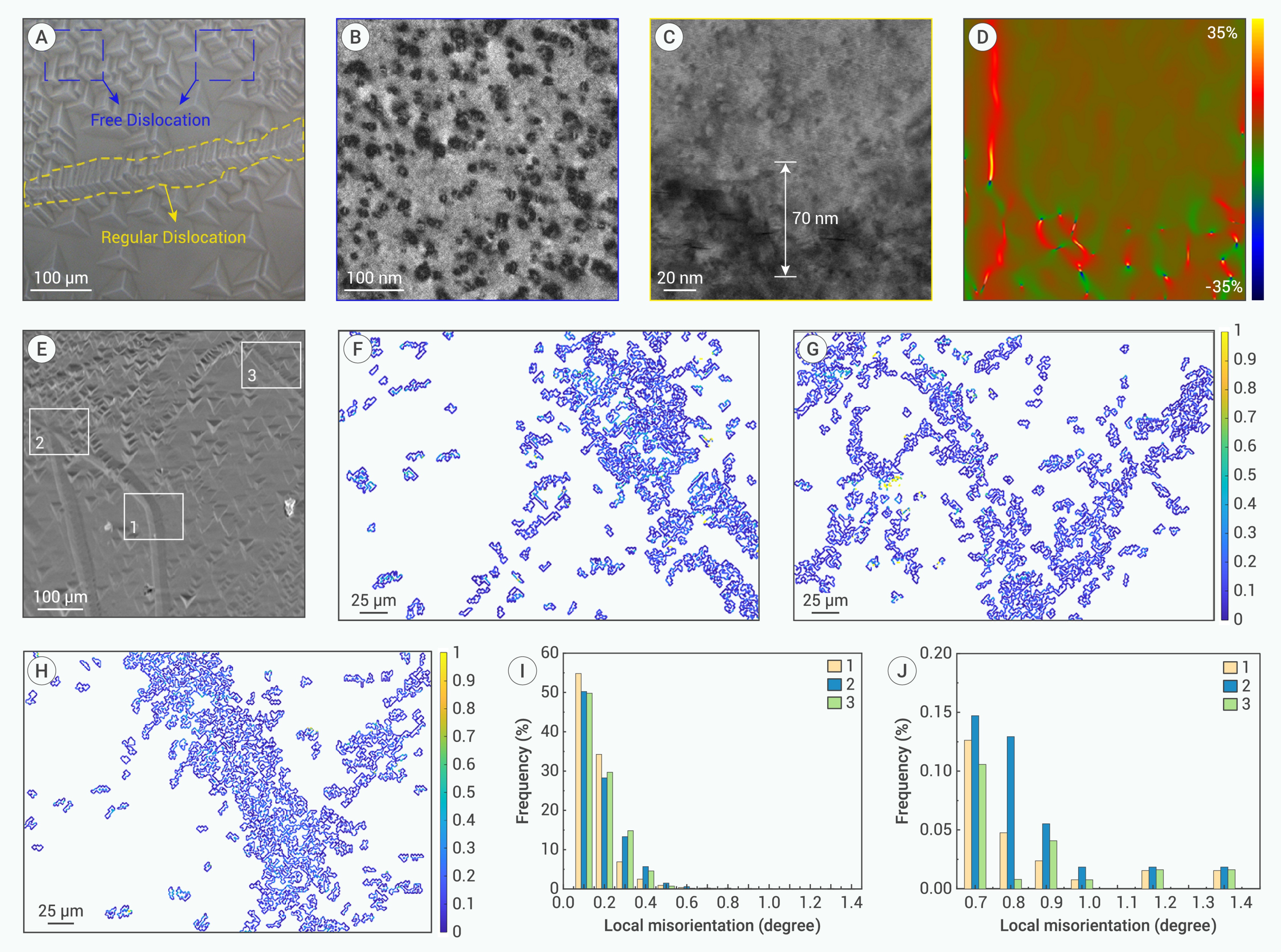
Figure 1.
Morphology, Distribution, and Stress Field Analysis of Dislocations in CaF2 Crystals
-
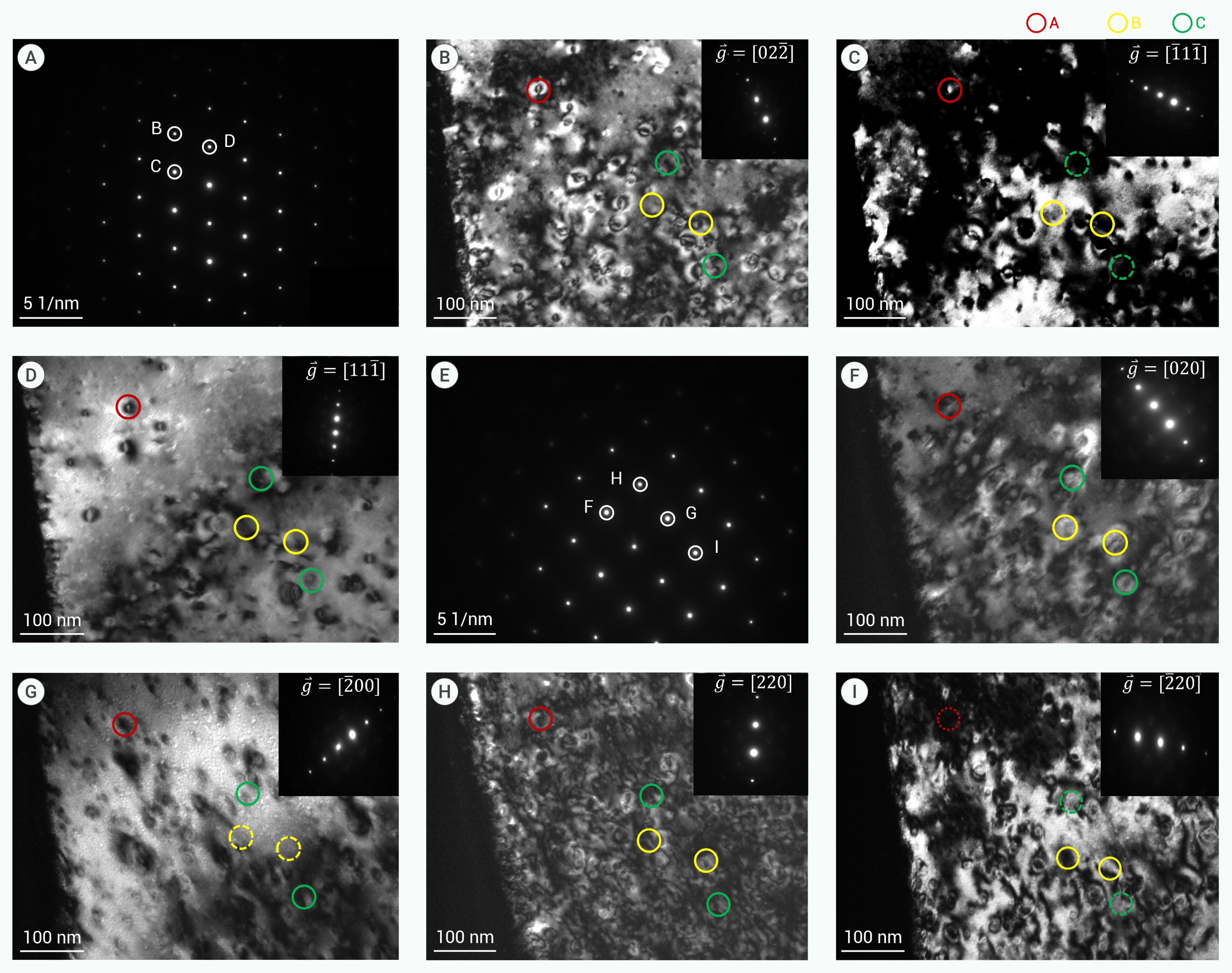
Figure 2.
Diffraction Contrast and Defect Imaging of CaF2 under Multiple Zone Axis and Diffraction Conditions
-
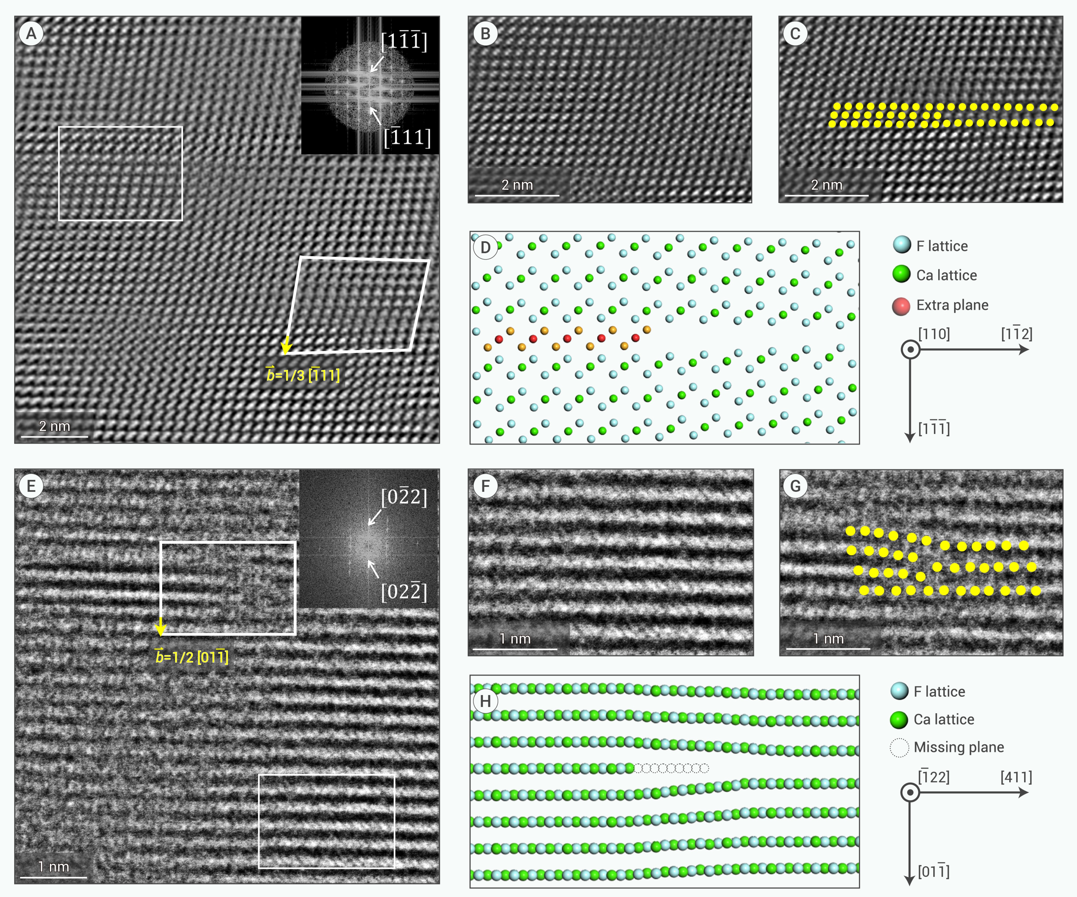
Figure 3.
Atomic-Scale Structure and Defect Configuration of Dislocations in CaF2 Crystals On-zone atomically resolved iDPC-STEM image of dislocations
-
Figure 4.
Atomic-scale characterization of GNDs in CaF2 crystals iDPC-STEM images of GNDs in CaF2
-
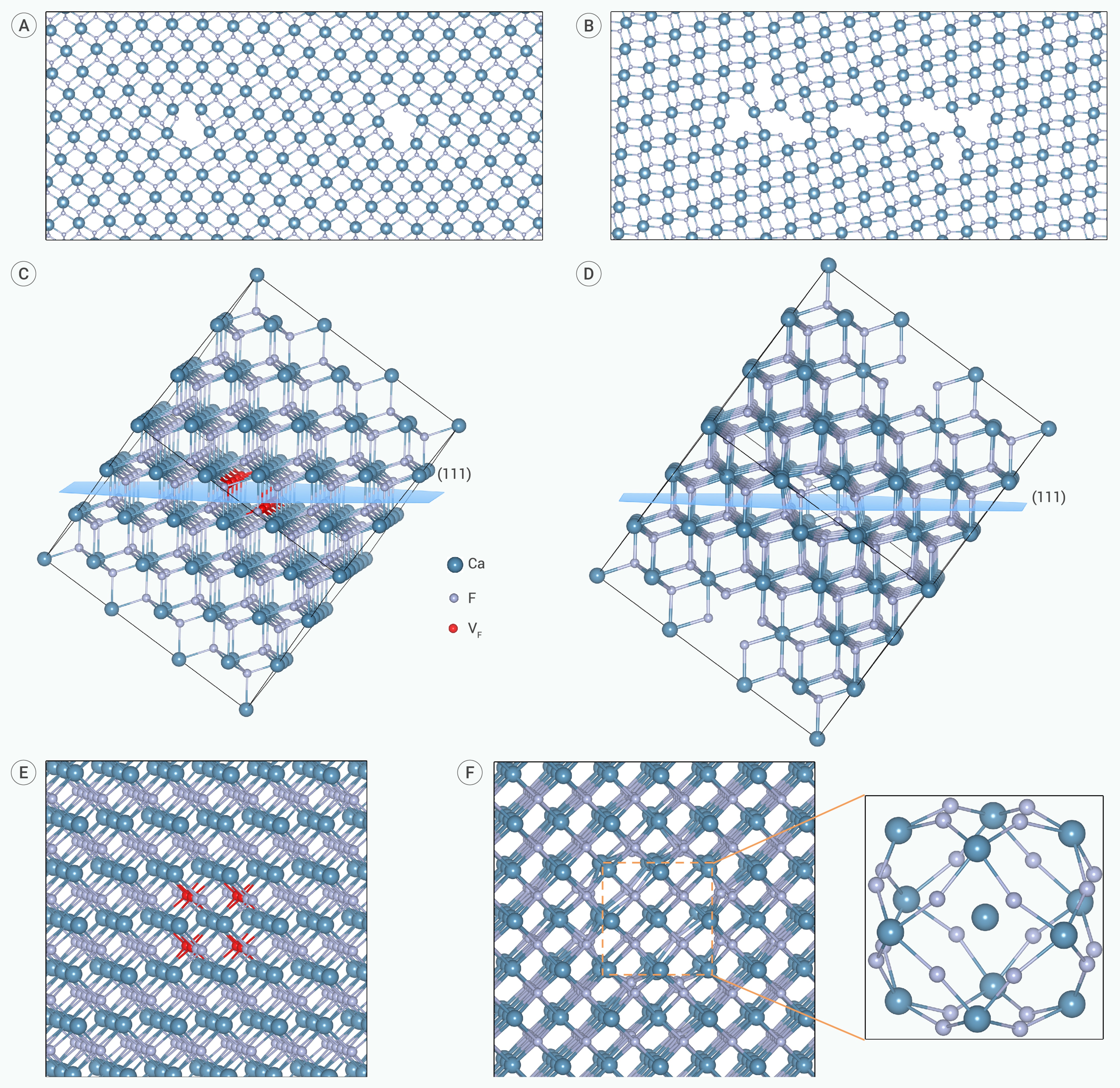
Figure 5.
Dislocation Core Structures and Fluorine Vacancy Evolution via Supercell Modeling
