
Nanoions tuned two-dimensional van der Waals materials for information devices
-
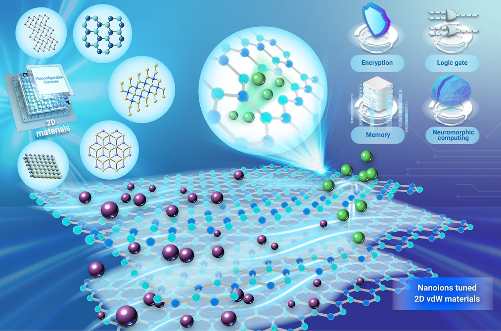
GRAPHICAL ABSTRACT
 DownLoad:
Full size image
DownLoad:
Full size image
-
PUBLIC SUMMARY
-
Nanoionics in two-dimensional (2D) materials and its impact on electrical properties are summarized.
Ion-driven 2D materials-based reconfigurable devices for information technology are discussed.
Opportunities for developing reconfigurable devices and expanding their multifunctionality are presented.
-
-
ABSTRACT
The rapid advancement of artificial intelligence (AI) and the Internet of Things (IoT) has triggered an escalating demand for high-performance, miniaturized, and multifunctional electronic information devices. Silicon-based electronics, which have laid the foundation for the electronics industry over the past few decades, are now approaching the physical limitations with the extension of Moore’s law. Two-dimensional (2D) van der Waals (vdW) materials have emerged as promising candidates for next-generation electronic devices, due to their atomic-scale thickness, wide range of material choices, and excellent physical property tunability. Notably, it has been demonstrated that 2D vdW materials can facilitate ion migration under an electric field, enabling the reversible and efficient modulation of electrical resistance. Such a characteristic unlocks new possibilities for the design and construction of multifunctional and reconfigurable information devices. This review delves into the generation and transport of nanoionics in 2D vdW materials and their impact on modifying electrical properties. It explores strategies for device architecture design and their applications in advanced information processing. The latest progress in ion-driven reconfigurable devices for memory, logic-in-memory, neuromorphic computing, and data encryption is systematically summarized. Challenges in this field and future research directions are also discussed. -

-
REFERENCES
[1] Pradhan D. K., Moore D. C., Francis A. M., et al. (2024). Materials for high-temperature digital electronics. Nat. Rev. Mater. 9:790−807. DOI:10.1038/s41578-024-00731-9 [2] Bardeen J. and Brattain W. H. (1948). The transistor, a semi-conductor triode. Phys. Rev. 74:230−231. DOI:10.1103/PhysRev.74.230 [3] Atalla M. M., Tannenbaum E. and Scheibner E. J. (1959). Stabilization of silicon surfaces by thermally grown oxides. Bell Syst. Tech. J. 38:749−783. DOI:10.1002/j.1538-7305.1959.tb03907.x [4] Kilby J. S. (1976). Invention of the integrated circuit. IEEE Trans. Electron Devices 23:648−654. DOI:10.1109/T-ED.1976.18467 [5] Chang L., Yang-kyu C., Ha D., et al. (2003). Extremely scaled silicon nano-CMOS devices. Proc. IEEE 91:1860−1873. DOI:10.1109/JPROC.2003.818336 [6] Davari B., Dennard R. H. and Shahidi G. G. (1995). CMOS scaling for high performance and low power-the next ten years. Proc. IEEE 83:595−606. DOI:10.1109/5.371968 [7] Cheng Z., Pang C.-S., Wang P., et al. (2022). How to report and benchmark emerging field-effect transistors. Nat. Electron. 5:416−423. DOI:10.1038/s41928-022-00798-8 [8] Syu J. H., Lin J. C. W., Srivastava G., et al. (2023). A comprehensive survey on artificial intelligence empowered edge computing on consumer electronics. IEEE Trans. Consum. Electron. 69:1023−1034. DOI:10.1109/TCE.2023.3318150 [9] Hua H., Li Y., Wang T., et al. (2023). Edge computing with artificial intelligence: A machine learning perspective. ACM Comput. Surv. 55:Article 184. DOI:10.1145/3555802. [10] Tsai C. W., Lai C. F., Chiang M. C., et al. (2014). Data mining for internet of things: A survey. IEEE Commun. Surv. Tutorials 16:77−97. DOI:10.1109/SURV.2013.103013.00206 [11] Mikolajick T., Heinzig A., Trommer J., et al. (2017). The RFET—a reconfigurable nanowire transistor and its application to novel electronic circuits and systems. Semicond. Sci. Technol. 32:043001. DOI:10.1088/1361-6641/aa5581 [12] Weber W. M., Heinzig A., Trommer J., et al. (2014). Reconfigurable nanowire electronics – A review. Solid-State Electron. 102:12−24. DOI:10.1016/j.sse.2014.06.010 [13] Zhu Z., Ng D. W. H., Park H. S., et al. (2021). 3D-printed multifunctional materials enabled by artificial-intelligence-assisted fabrication technologies. Nat. Rev. Mater. 6:27−47. DOI:10.1038/s41578-020-00235-2 [14] Rai S., Trommer J., Raitza M., et al. (2019). Designing efficient circuits based on runtime-reconfigurable field-effect transistors. IEEE Trans. Very Large Scale Integr. VLSI Syst. 27:560−572. DOI:10.1109/TVLSI.2018.2884646 [15] Qiu E., Zhang Y.-H., Ventra M. D., et al. (2024). Reconfigurable cascaded thermal neuristors for neuromorphic computing. Adv. Mater. 36:2306818. DOI:10.1002/adma.202306818 [16] Zhu J., Dexheimer M. and Cheng H. (2017). Reconfigurable systems for multifunctional electronics. npj Flex. Electron. 1:8. DOI:10.1038/s41528-017-0009-6 [17] Chen C. K., Hooda S., Fang Z., et al. (2023). High-performance top-gated and double-gated oxide–semiconductor ferroelectric field-effect transistor enabled by channel defect self-compensation effect. IEEE Trans. Electron Devices 70:2098−2105. DOI:10.1109/TED.2023.3242633 [18] Lundstrom M. (2003). Moore's law forever. Science 299:210−211. DOI:10.1126/science.1079567 [19] Zidan M. A., Strachan J. P. and Lu W. D. (2018). The future of electronics based on memristive systems. Nat. Electron. 1:22−29. DOI:10.1038/s41928-017-0006-8 [20] Tan C., Tang J., Gao X., et al. (2025). 2D bismuth oxyselenide semiconductor for future electronics. Nat. Rev. Electr. Eng. 2:494−513. DOI:10.1038/s44287-025-00179-1 [21] Ataca C., Şahin H. and Ciraci S. (2012). Stable, single-layer MX2 transition-metal oxides and dichalcogenides in a honeycomb-like structure. J. Phys. Chem. C 116:8983−8999. DOI:10.1021/jp212558p [22] Pang J., Zhang S., Rümmeli M. H., et al. (2023). Evolving MXene species. Innov. Mater. 1:100027. DOI:10.59717/j.xinn-mater.2023.100027 [23] Huh W., Lee D. and Lee C.-H. (2020). Memristors based on 2D materials as an artificial synapse for neuromorphic electronics. Adv. Mater. 32:2002092. DOI:10.1002/adma.202002092 [24] Kim K., Choi J.-Y., Kim T., et al. (2011). A role for graphene in silicon-based semiconductor devices. Nature 479:338−344. DOI:10.1038/nature10680 [25] Zou X., Xu Y. and Duan W. (2021). 2D materials: Rising star for future applications. The Innovation 2. DOI:10.1016/j.xinn.2021.100115 [26] Serles P., Arif T., Puthirath A. B., et al. Friction of magnetene, a non–van der Waals 2D material. Sci. Adv. 7:eabk2041. DOI:10.1126/sciadv.abk2041 [27] Turunen M., Brotons-Gisbert M., Dai Y., et al. (2022). Quantum photonics with layered 2D materials. Nat. Rev. Phys. 4:219−236. DOI:10.1038/s42254-021-00408-0 [28] Favron A., Gaufrès E., Fossard F., et al. (2015). Photooxidation and quantum confinement effects in exfoliated black phosphorus. Nat. Mater. 14:826−832. DOI:10.1038/nmat4299 [29] Nakamura K., Nagamura N., Ueno K., et al. (2020). All 2D heterostructure tunnel field-effect transistors: Impact of band alignment and heterointerface quality. ACS Appl. Mater. Interfaces 12:51598−51606. DOI:10.1021/acsami.0c13233 [30] Ben Jabra Z., Abel M., Fabbri F., et al. (2022). Van der Waals heteroepitaxy of air-stable quasi-free-standing silicene layers on CVD epitaxial graphene/6H-SiC. ACS Nano 16:5920−5931. DOI:10.1021/acsnano.1c11122 [31] Diallo T. M., Hanuš T., Patriarche G., et al. (2024). Unraveling the heterointegration of 3D semiconductors on graphene by anchor point nucleation. Small 20:2306038. DOI:10.1002/smll.202306038 [32] Liu Y., Duan X., Huang Y., et al. (2018). Two-dimensional transistors beyond graphene and TMDCs. Chem. Soc. Rev. 47:6388−6409. DOI:10.1039/C8CS00318A [33] Ng H. K., Xiang D., Suwardi A., et al. (2022). Improving carrier mobility in two-dimensional semiconductors with rippled materials. Nat. Electron. 5:489−496. DOI:10.1038/s41928-022-00777-z [34] Zeng S., Liu C. and Zhou P. (2024). Transistor engineering based on 2D materials in the post-silicon era. Nat. Rev. Electr. Eng. 1:335−348. DOI:10.1038/s44287-024-00045-6 [35] Butler S. Z., Hollen S. M., Cao L., et al. (2013). Progress, challenges, and opportunities in two-dimensional materials beyond graphene. ACS Nano 7:2898−2926. DOI:10.1021/nn400280c [36] Xie L., Liao M., Wang S., et al. (2017). Graphene-contacted ultrashort channel monolayer MoS2 transistors. Adv. Mater. 29:1702522. DOI:10.1002/adma.201702522 [37] Cheng Z., Backman J., Zhang H., et al. (2023). Distinct contact scaling effects in MoS2 transistors revealed with asymmetrical contact measurements. Adv. Mater. 35:2210916. DOI:10.1002/adma.202210916 [38] Zhao W., Ghorannevis Z., Chu L., et al. (2013). Evolution of electronic structure in atomically thin sheets of WS2 and WSe2. ACS Nano 7:791−797. DOI:10.1021/nn305275h [39] Li L., Deng Q., Sun Y., et al. (2023). 2D short-channel tunneling transistor relying on dual-gate modulation for integrated circuits application. Adv. Funct. Mater. 33:2304591. DOI:10.1002/adfm.202304591 [40] Deng Q., Zhao T., Zhang J., et al. (2024). Reconfigurable vertical phototransistor with MoTe2 homojunction for high-speed rectifier and multivalued logical circuits. ACS Nano 18:23702−23710. DOI:10.1021/acsnano.4c08345 [41] Zhu Y., Long R. and Fang W.-H. (2023). Substrate ferroelectric proximity effects have a strong influence on charge carrier lifetime in black phosphorus. Nano Lett. 23:10074−10080. DOI:10.1021/acs.nanolett.3c03570 [42] Namgung S., Koester S. J. and Oh S.-H. (2021). Ultraflat sub-10 nanometer gap electrodes for two-dimensional optoelectronic devices. ACS Nano 15:5276−5283. DOI:10.1021/acsnano.0c10759 [43] Bandurin D. A., Tyurnina A. V., Yu G. L., et al. (2017). High electron mobility, quantum Hall effect and anomalous optical response in atomically thin InSe. Nat. Nanotechnol. 12:223−227. DOI:10.1038/nnano.2016.242 [44] Xiang Y., Wang C., Liu C., et al. (2025). Subnanosecond flash memory enabled by 2D-enhanced hot-carrier injection. Nature 641:90−97. DOI:10.1038/s41586-025-08839-w [45] Wang Z., Liu X., Zhou X., et al. (2022). Reconfigurable quasi-nonvolatile memory/subthermionic FET functions in ferroelectric–2D semiconductor vdW architectures. Adv. Mater. 34:2200032. DOI:10.1002/adma.202200032 [46] Yang J. Y., Park M., Yeom M. J., et al. (2023). Reconfigurable physical reservoir in GaN/α-In2Se3 HEMTs enabled by out-of-plane local polarization of ferroelectric 2D layer. ACS Nano 17:7695−7704. DOI:10.1021/acsnano.3c00187 [47] Li C., Tian R., Chen X., et al. (2022). Waveguide-integrated MoTe2 p–i–n homojunction photodetector. ACS Nano 16:20946−20955. DOI:10.1021/acsnano.2c08549 [48] Wang P., Mu H., Yun T., et al. (2025). High rectification and gate-tunable photoresponse in 1D-2D lateral van der Waals heterojunctions. Innov. Mater. 3:100113. DOI:10.59717/j.xinn-mater.2024.100113 [49] Jiang J., Xu L., Qiu C., et al. (2023). Ballistic two-dimensional InSe transistors. Nature 616:470−475. DOI:10.1038/s41586-023-05819-w [50] Tan C., Yu M., Tang J., et al. (2023). 2D fin field-effect transistors integrated with epitaxial high-k gate oxide. Nature 616:66−72. DOI:10.1038/s41586-023-05797-z [51] Fei W., Trommer J., Lemme M. C., et al. (2022). Emerging reconfigurable electronic devices based on two-dimensional materials: A review. InfoMat 4:e12355. DOI:10.1002/inf2.12355 [52] Zhang J., Liu W., Dai J., et al. (2022). Nanoionics from biological to artificial systems: An alternative beyond nanoelectronics. Adv. Sci. 9:2200534. DOI:10.1002/advs.202200534 [53] Yang Y., Wang M., He Q., et al. (2025). Ion transport behavior in van der Waals Gaps of 2D materials. Small 21:2310681. DOI:10.1002/smll.202310681 [54] Liao K., Chen L., Meng R., et al. (2024). Reconstructable carbon monolayer-MoS2 intercalated heterostructure enabled by atomic layers-confined topotactic transformation for ultrafast lithium storage. J. Am. Chem. Soc. 146:12020−12029. DOI:10.1021/jacs.4c01550 [55] Shi W., Kahn S., Jiang L., et al. (2020). Reversible writing of high-mobility and high-carrier-density doping patterns in two-dimensional van der Waals heterostructures. Nat. Electron. 3:99−105. DOI:10.1038/s41928-019-0351-x [56] Kim T., Won J., Bae J., et al. (2025). Memristive InAs-based semiconductors with anisotropic ion transport. Adv. Mater. 37:2500056. DOI:10.1002/adma.202500056 [57] Muscher P. K., Rehn D. A., Sood A., et al. (2021). Highly efficient uniaxial in-plane stretching of a 2D material via ion insertion. Adv. Mater. 33:2101875. DOI:10.1002/adma.202101875 [58] Park H., Lee M., Wang X., et al. (2024). Anisotropic charge transport at the metallic edge contact of ReS2 field effect transistors. Commun. Mater. 5:87. DOI:10.1038/s43246-024-00526-z [59] Sun P., Ma R. and Sasaki T. (2018). Recent progress on exploring exceptionally high and anisotropic H+/OH− ion conduction in two-dimensional materials. Chem. Sci. 9:33−43. DOI:10.1039/C7SC04019A [60] Ram A., Maity K., Marchand C., et al. (2023). Reconfigurable multifunctional van der Waals ferroelectric devices and logic circuits. ACS Nano 17:21865−21877. DOI:10.1021/acsnano.3c07952 [61] Uzhansky M., Mukherjee S., Vijayan G., et al. (2024). Non-volatile reconfigurable p–n junction utilizing in-plane ferroelectricity in 2D WSe2/α-In2Se3 asymmetric heterostructures. Adv. Funct. Mater. 34:2306682. DOI:10.1002/adfm.202306682 [62] Mei T., Chen F., Huang T., et al. (2025). Ion–electron interactions in 2D nanomaterials-based artificial synapses for neuromorphic applications. ACS Nano 19:17140−17172. DOI:10.1021/acsnano.5c02397 [63] Yang Q., Li X., Zhao L., et al. (2025). Unified transmission electron microscopy with the glovebox integrated system for investigating air-sensitive two-dimensional quantum materials. The Innovation 6:100751. DOI:10.1016/j.xinn.2024.100751 [64] Li W., Qian X. and Li J. (2021). Phase transitions in 2D materials. Nat. Rev. Mater. 6:829−846. DOI:10.1038/s41578-021-00304-0 [65] Nirmal K. A., Kumbhar D. D., Kesavan A. V., et al. (2024). Advancements in 2D layered material memristors: Unleashing their potential beyond memory. npj 2D Mater. Appl. 8:83. DOI:10.1038/s41699-024-00522-4 [66] Jiang J., Xu T., Lu J., et al. Defect engineering in 2D materials: Precise manipulation and improved functionalities. Research 2019. DOI:10.34133/2019/4641739 [67] Papadopoulos S., Agarwal T., Jain A., et al. (2022). Ion migration in monolayer MoS2 memristors. Phys. Rev. Appl. 18:014018. DOI:10.1103/PhysRevApplied.18.014018 [68] Ghorbani-Asl M., Kretschmer S., Spearot D. E., et al. (2017). Two-dimensional MoS2 under ion irradiation: From controlled defect production to electronic structure engineering. 2D Mater. 4:025078. DOI:10.1088/2053-1583/aa6b17 [69] Teja Nibhanupudi S. S., Roy A., Veksler D., et al. (2024). Ultra-fast switching memristors based on two-dimensional materials. Nat. Commun. 15:2334. DOI:10.1038/s41467-024-46372-y [70] Wang M., Cai S., Pan C., et al. (2018). Robust memristors based on layered two-dimensional materials. Nat. Electron. 1:130−136. DOI:10.1038/s41928-018-0021-4 [71] Chen S., Mahmoodi M. R., Shi Y., et al. (2020). Wafer-scale integration of two-dimensional materials in high-density memristive crossbar arrays for artificial neural networks. Nat. Electron. 3:638−645. DOI:10.1038/s41928-020-00473-w [72] Lee G. S., Kim J. G., Kim J. T., et al. (2024). 2D materials beyond post-AI era: Smart fibers, soft robotics, and single atom catalysts. Adv. Mater. 36:2307689. DOI:10.1002/adma.202307689 [73] Pomerantseva E. and Gogotsi Y. (2017). Two-dimensional heterostructures for energy storage. Nat. Energy 2:17089. DOI:10.1038/nenergy.2017.89 [74] Shifa T. A., Wang F., Liu Y., et al. (2019). Heterostructures based on 2D materials: A versatile platform for efficient catalysis. Adv. Mater. 31:1804828. DOI:10.1002/adma.201804828 [75] Zhou F., Chen J., Tao X., et al. 2D materials based optoelectronic memory: Convergence of electronic memory and optical sensor. Research 2019. DOI:10.34133/2019/9490413 [76] Ci W., Wang P., Xue W., et al. (2024). Engineering ferroelectric-/ion-modulated conductance in 2D vdW CuInP2S6 for non-volatile digital memory and artificial synapse. Adv. Funct. Mater. 34:2316360. DOI:10.1002/adfm.202316360 [77] Chen J., Zhu C., Cao G., et al. (2022). Mimicking neuroplasticity via ion migration in van der Waals layered copper indium thiophosphate. Adv. Mater. 34:2104676. DOI:10.1002/adma.202104676 [78] Lee M. J., Kim S.-H., Lee S., et al. (2020). Understanding filamentary growth and rupture by Ag ion migration through single-crystalline 2D layered CrPS4. NPG Asia Mater. 12:82. DOI:10.1038/s41427-020-00272-x [79] Zabelotsky T., Singh S., Haim G., et al. (2023). Creation of boron vacancies in hexagonal boron nitride exfoliated from bulk crystals for quantum sensing. ACS Appl. Nano Mater. 6:21671−21678. DOI:10.1021/acsanm.3c03395 [80] Kang C., Choi H., Son H., et al. (2023). A steep-switching impact ionization-based threshold switching field-effect transistor. Nanoscale 15:5771−5777. DOI:10.1039/D2NR06547A [81] Marques-Moros F., Boix-Constant C., Mañas-Valero S., et al. (2023). Interplay between optical emission and magnetism in the van der Waals magnetic semiconductor CrSBr in the two-dimensional limit. ACS Nano 17:13224−13231. DOI:10.1021/acsnano.3c00375 [82] Ma M. Y., Chen N. K., Wang D., et al. (2023). Defect physics in 2D monolayer I-VII semiconductor AgI. Mater. Today Nano 22:100304. DOI:10.1016/j.mtnano.2023.100304 [83] Jiang X., Zhang X., Deng Z., et al. (2024). Dual-role ion dynamics in ferroionic CuInP2S6: Revealing the transition from ferroelectric to ionic switching mechanisms. Nat. Commun. 15:10822. DOI:10.1038/s41467-024-55160-7 [84] Sun Y., Zhang R., Teng C., et al. (2023). Internal ion transport in ionic 2D CuInP2S6 enabling multi-state neuromorphic computing with low operation current. Mater. Today 66:9−16. DOI:10.1016/j.mattod.2023.04.013 [85] Guo C., Zhu J., Liang X., et al. (2024). Atomic-level direct imaging for Cu(I) multiple occupations and migration in 2D ferroelectric CuInP2S6. Nat. Commun. 15:10152. DOI:10.1038/s41467-024-54229-7 [86] Malik A. M., Albe K. and Rohrer J. (2025). Vacancy formation energy as a descriptor of the exfoliability of MAX phases to MXenes. npj 2D Mater. Appl. 9:56. DOI:10.1038/s41699-025-00581-1 [87] Li Z. and Chen F. (2017). Ion beam modification of two-dimensional materials: Characterization, properties, and applications. Appl. Phys. Rev. 4:011103. DOI:10.1063/1.4977087 [88] Qi Y., Sadi M. A., Hu D., et al. (2023). Recent progress in strain engineering on van der Waals 2D materials: Tunable electrical, electrochemical, magnetic, and optical properties. Adv. Mater. 35:2205714. DOI:10.1002/adma.202205714 [89] Du S., Yang W., Gao H., et al. (2024). Sliding memristor in parallel-stacked hexagonal boron nitride. Adv. Mater. 36:2404177. DOI:10.1002/adma.202404177 [90] Qin L., Yu Y., Fang C., et al. (2025). Intrinsic ion migration-induced susceptible two-dimensional phase-transition memristor with ultralow power consumption. Sci. Bull. 70:2116−2124. DOI:10.1016/j.scib.2025.03.051 [91] Chen W., Wang Z., Bets K. V., et al. (2021). Millisecond conversion of metastable 2D materials by flash Joule heating. ACS Nano 15:1282−1290. DOI:10.1021/acsnano.0c08460 [92] Yang S.-Z., Sun W., Zhang Y.-Y., et al. (2019). Direct cation exchange in monolayer MoS2 via recombination-enhanced migration. Phys. Rev. Lett. 122:106101. DOI:10.1103/PhysRevLett.122.106101 [93] Yang X., Luo Y., Li J., et al. (2022). Tuning mixed electronic/ionic conductivity of 2D CdPS3 nanosheets as an anode material by synergistic intercalation and vacancy engineering. Adv. Funct. Mater. 32:2112169. DOI:10.1002/adfm.202112169 [94] Zheng J., Zhang H., Dong S., et al. (2014). High yield exfoliation of two-dimensional chalcogenides using sodium naphthalenide. Nat. Commun. 5:2995. DOI:10.1038/ncomms3995 [95] Li J., Ge X., Liang Q., et al. (2024). Quantitative pre-intercalation of alkali metal ions enables precisely modulating Li+ storage of MXenes. Energy Storage Mater. 73. 103828,DOI:10.1016/j.ensm.2024.103828. [96] Zhao Y., Chen D., Deng Z., et al. (2025). Stacking-dependent ion adsorption and diffusion in Janus MoSSe bilayers: Insights for battery applications. J. Power Sources 641:236855. DOI:10.1016/j.jpowsour.2025.236855 [97] Zhang H., Koledin T. D., Wang X., et al. (2022). Stabilizing the heavily-doped and metallic phase of MoS2 monolayers with surface functionalization. 2D Mater. 9:015033. DOI:10.1088/2053-1583/ac3f44. [98] Stephenson T., Li Z., Olsen B., et al. (2014). Lithium ion battery applications of molybdenum disulfide (MoS2) nanocomposites. Energy Environ. Sci. 7:209−231. DOI:10.1039/C3EE42591F [99] Zhu Q., Li W., Wu J., et al. (2022). Vacancy engineering in WS2 nanosheets for enhanced potassium‐ion storage. J. Power Sources 542:231791. DOI:10.1016/j.jpowsour.2022.231791 [100] Luo X., Huang J., Cao L., et al. (2023). Constructing multi-dimensional migration channel by nickel-doped WS2 composite: High speed sodium and potassium ion storage kinetics in WS2 nanosheets. Chem. Eng. J. 464:142579. DOI:10.1016/j.cej.2023.142579 [101] Yang R., Mei L., Lin Z., et al. (2024). Intercalation in 2D materials and in situ studies. Nat. Rev. Chem. 8:410−432. DOI:10.1038/s41570-024-00605-2 [102] Chen Q., Wei Y., Zhai P.-B., et al. (2024). Van der Waals gap engineering in 2D materials for energy storage and conversion. Rare Met. 43:6125−6143. DOI:10.1007/s12598-024-02817-3 [103] Ghosh K., Ng S., Lazar P., et al. (2024). 2D germanane-MXene heterostructures for cations intercalation in energy storage applications. Adv. Funct. Mater. 34:2308793. DOI:10.1002/adfm.202308793 [104] Fernandes J., Grzonka J., Araújo G., et al. (2024). Bipolar resistive switching in 2D MoSe2 grown by atmospheric pressure chemical vapor peposition. ACS Appl. Mater. Interfaces 16:1767−1778. DOI:10.1021/acsami.3c14215 [105] Xu R., Jang H., Lee M.-H., et al. (2019). Vertical MoS2 double-layer memristor with electrochemical metallization as an atomic-scale synapse with switching thresholds approaching 100 mV. Nano Lett. 19:2411−2417. DOI:10.1021/acs.nanolett.8b05140 [106] Khot A. C., Dongale T. D., Nirmal K. A., et al. (2022). Amorphous boron nitride memristive device for high-density memory and neuromorphic computing applications. ACS Appl. Mater. Interfaces 14:10546−10557. DOI:10.1021/acsami.1c23268 [107] Yin S., Luo Z., Li Q., et al. (2019). Emulation of learning and memory behaviors by memristor based on Ag migration on 2D MoS2 surface. Phys. Status Solidi A 216:1900104. DOI:10.1002/pssa.201900104 [108] Li C., Xu T., Pan R., et al. (2024). Electric field-dependent evolution dynamics of conductive filaments in 2D material-based planar memristors. ACS Nano 18:32196−32204. DOI:10.1021/acsnano.4c11598 [109] Mitra S. and Mahapatra S. (2024). Atomistic description of conductive bridge formation in two-dimensional material based memristor. npj 2D Mater. Appl. 8:26. DOI:10.1038/s41699-024-00465-w [110] Boland M. J., Sundararajan A., Farrokhi M. J., et al. (2016). Nonlinear ballistic transport in an atomically thin material. ACS Nano 10:1231−1239. DOI:10.1021/acsnano.5b06546 [111] Lee C. H., Park Y., Youn S., et al. (2022). Design of p-WSe2/n-Ge heterojunctions for high-speed broadband photodetectors. Adv. Funct. Mater. 32:2107992. DOI:10.1002/adfm.202107992 [112] Zhou Y., Zhang C., Huang D., et al. (2022). Structure defined 2D Mo2C/2Dg-C3N4 van der Waals heterojunction: Oriented charge flow in-plane and separation within the interface to collectively promote photocatalytic degradation of pharmaceutical and personal care products. Appl. Catal., B 301:120749. DOI:10.1016/j.apcatb.2021.120749 [113] Waser R., Dittmann R., Staikov G., et al. (2009). Redox-based resistive switching memories – nanoionic mechanisms, prospects, and challenges. Adv. Mater. 21:2632−2663. DOI:10.1002/adma.200900375 [114] Waser R. and Aono M. (2007). Nanoionics-based resistive switching memories. Nat. Mater. 6:833−840. DOI:10.1038/nmat2023 [115] Han S. S., Shawkat M. S., Lee Y. H., et al. (2022). Wafer-scale anion exchange conversion of nonlayered PtS films to van der Waals two-dimensional PtTe2 layers with negative photoresponsiveness. Chem. Mater. 34:6996−7005. DOI:10.1021/acs.chemmater.2c01452 [116] Du L., Hasan T., Castellanos-Gomez A., et al. (2021). Engineering symmetry breaking in 2D layered materials. Nat. Rev. Phys. 3:193−206. DOI:10.1038/s42254-020-00276-0 [117] Xiao Y., Zhou M., Zeng M., et al. (2019). Atomic-scale structural modification of 2D materials. Adv. Sci. 6:1801501. DOI:10.1002/advs.201801501 [118] Kim S., Cui J., Dravid V. P., et al. (2019). Orientation-dependent intercalation channels for lithium and sodium in black phosphorus. Adv. Mater. 31:1904623. DOI:10.1002/adma.201904623 [119] Xiang P., Chen X., Zhang W., et al. (2017). Metallic borophene polytypes as lightweight anode materials for non-lithium-ion batteries. Phys. Chem. Chem. Phys. 19:24945−24954. DOI:10.1039/C7CP04989G [120] Ueda A., Zhang Y., Sano N., et al. (2020). Ambipolar device simulation based on the drift-diffusion model in ion-gated transition metal dichalcogenide transistors. npj Comput. Mater. 6:24. DOI:10.1038/s41524-020-0293-x [121] Xu X., Chen Y., Liu P., et al. (2024). General synthesis of ionic-electronic coupled two-dimensional materials. Nat. Commun. 15:4368. DOI:10.1038/s41467-024-48690-7 [122] Ge R., Wu X., Liang L., et al. (2021). A library of atomically thin 2D materials featuring the conductive-point resistive switching phenomenon. Adv. Mater. 33:2007792. DOI:10.1002/adma.202007792 [123] Zhu H., Li J., Chen Q., et al. (2023). Highly tunable lateral homojunction formed in two-dimensional layered CuInP2S6 via in-plane ionic migration. ACS Nano 17:1239−1246. DOI:10.1021/acsnano.2c09280 [124] Ni S., Jiang J., Wang W., et al. (2025). Beryllium dinitride monolayer: A multifunctional direct bandgap anisotropic semiconductor containing polymeric nitrogen with oxygen reduction catalysis and potassium-ion storage capability. J. Mater. Chem. A 13:10214−10223. DOI:10.1039/D4TA08565E [125] Sun Y., Zhang R., Tan J., et al. Tunable in-plane conductance anisotropy in 2D semiconductive AgCrP2S6 by ion-electron co-modulations. Sci. Adv. 11:eadr3105. DOI:10.1126/sciadv.adr3105 [126] Liu H., Zhang Y., Glukhova O. E., et al. (2022). Interlayer hopping kinetics of vacancies in CrI3 layers leading to monolayer/bilayer heterostructures. Adv. Mater. Interfaces 9:2200626. DOI:10.1002/admi.202200626 [127] Shen T., Li F., Xu L., et al. (2020). High mobility monolayer MoS2 transistors and its charge transport behaviour under E-beam irradiation. J. Mater. Sci. 55:14315−14325. DOI:10.1007/s10853-020-04977-w [128] Olsson E., Hussain T., Karton A., et al. (2020). The adsorption and migration behavior of divalent metals (Mg, Ca, and Zn) on pristine and defective graphene. Carbon 163:276−287. DOI:10.1016/j.carbon.2020.03.028 [129] Wang Z., Chen J., Cao Z., et al. (2025). First-principles study of anionic diffusion in two-dimensional lead halide perovskite lateral heterostructures. ACS Appl. Mater. Interfaces 17:7019−7026. DOI:10.1021/acsami.4c11155 [130] Sangwan V. K., Jariwala D., Kim I. S., et al. (2015). Gate-tunable memristive phenomena mediated by grain boundaries in single-layer MoS2. Nat. Nanotechnol. 10:403−406. DOI:10.1038/nnano.2015.56 [131] Lee D. J., Lee Y., Hong C.-W., et al. (2021). Liquid-to-solid exfoliated Ag/2D-SnO/Au flexible memristor with electric field direction-dependent asymmetric hysteresis characteristics. J. Mater. Res. Technol. 15:3538−3546. DOI:10.1016/j.jmrt.2021.09.147 [132] Wu H., Guo Z., Zhou J., et al. (2019). Vacancy-mediated lithium adsorption and diffusion on MXene. Appl. Surf. Sci. 488:578−585. DOI:10.1016/j.apsusc.2019.05.311 [133] Wang G., Luo X., Chen C., et al. (2023). Defect-engineered hexagonal boron nitride nanosheets as a new atomic-level directional ion conductor. Ceram. Int. 49:23391−23398. DOI:10.1016/j.ceramint.2023.04.171 [134] Yoo J., Nam C.-Y. and Bussmann E. (2024). Atomic precision processing of two-dimensional materials for next-generation microelectronics. ACS Nano 18:21614−21622. DOI:10.1021/acsnano.4c04908 [135] Zhang H. (2018). Introduction: 2D materials chemistry. Chem. Rev. 118:6089−6090. DOI:10.1021/acs.chemrev.8b00278 [136] Pushkarev G. V., Mazurenko V. G., Mazurenko V. V., et al. (2023). Nature of interlayer bonds in two-dimensional materials. J. Phys. Chem. C 127:8148−8158. DOI:10.1021/acs.jpcc.3c01248 [137] Zhou J., Chen A., Zhang Y., et al. (2023). 2D ferroionics: Conductive switching mechanisms and transition boundaries in van der Waals layered material CuInP2S6. Adv. Mater. 35:2302419. DOI:10.1002/adma.202302419 [138] Yang Y., Wang M., He Q., et al. (2025). Ion transport behavior in van der Waals gaps of 2D materials. Small 21:2310681. DOI:10.1002/smll.202310681 [139] Li Y., Xiong Y., Zhang X., et al. (2024). Memristors with analogue switching and high on/off ratios using a van der Waals metallic cathode. Nat. Electron. 8:36−45. DOI:10.1038/s41928-024-01269-y [140] Kretschmer S., Ghaderzadeh S., Facsko S., et al. (2022). Threshold ion energies for creating defects in 2D materials from first-principles calculations: Chemical interactions are important. J. Phys. Chem. Lett. 13:514−519. DOI:10.1021/acs.jpclett.1c03995 [141] Lee J., Du C., Sun K., et al. (2016). Tuning ionic transport in memristive devices by graphene with engineered nanopores. ACS Nano 10:3571−3579. DOI:10.1021/acsnano.5b07943 [142] Kitsios S., Bousoulas P., Spithouris D., et al. (2022). Demonstration of enhanced switching variability and conductance quantization properties in a SiO2 conducting bridge resistive memory with embedded two-dimensional MoS2 material. ACS Appl. Electron. Mater. 4:2869−2878. DOI:10.1021/acsaelm.2c00362 [143] Kang Y., Zhai X., Yang Q., et al. (2025). Conductive dendrite engineering of single-crystalline two-dimensional dielectric memristors. The Innovation 6:100885. DOI:10.1016/j.xinn.2025.100885 [144] Nessralla J., Larson D. T., Taniguchi T., et al. (2023). Modulating the electrochemical intercalation of graphene interfaces with α-RuCl3 as a solid-state electron acceptor. Nano Lett. 23:10334−10341. DOI:10.1021/acs.nanolett.3c02877 [145] Liu Q., Lin Y.-C., Kretschmer S., et al. (2023). Molybdenum chloride nanostructures with giant lattice distortions intercalated into bilayer graphene. ACS Nano 17:23659−23670. DOI:10.1021/acsnano.3c06958 [146] Hao Z., Chen J., Zhao Q., et al. (2025). Phase transformation induced basal plane capacitance enhancement in two-dimensional materials for electro-driven ion capture. Nano Lett. 25:6753−6761. DOI:10.1021/acs.nanolett.5c00982 [147] Kappera R., Voiry D., Yalcin S. E., et al. (2014). Phase-engineered low-resistance contacts for ultrathin MoS2 transistors. Nat. Mater. 13:1128−1134. DOI:10.1038/nmat4080 [148] Cho S., Kim S., Kim J. H., et al. (2015). Phase patterning for ohmic homojunction contact in MoTe2. Science 349:625−628. DOI:10.1126/science.aab3175 [149] Yang H., Huang H., Liu X., et al. (2023). Sensing mechanism of an Au-TiO2-Ag nanograting based on Fano resonance effects. Appl. Opt. 62:4431−4438. DOI:10.1364/AO.491732 [150] Guan J., Shao L., Yu L., et al. (2022). Two-dimensional Mg0.2V2O5·nH2O nanobelts derived from V4C3 MXenes for highly stable aqueous zinc ion batteries. Chem. Eng. J. 443:136502. DOI:10.1016/j.cej.2022.136502. [151] Rajapakse M., Karki B., Abu U. O., et al. (2021). Intercalation as a versatile tool for fabrication, property tuning, and phase transitions in 2D materials. npj 2D Mater. Appl. 5:30. DOI:10.1038/s41699-021-00211-6 [152] Hossain A. K. M. M., McBride J., Mahmoudi Gahrouei M., et al. (2025). Intercalation-induced topotactic phase transformation of tungsten disulfide crystals. Chem. Mater. 37:129−138. DOI:10.1021/acs.chemmater.4c02160 [153] Li Y., Yan H., Xu B., et al. (2021). Electrochemical intercalation in atomically thin van der Waals materials for structural phase transition and device applications. Adv. Mater. 33:2000581. DOI:10.1002/adma.202000581 [154] Lv R., Robinson J. A., Schaak R. E., et al. (2015). Transition metal dichalcogenides and beyond: synthesis, properties, and applications of single- and few-layer nanosheets. Acc. Chem. Res. 48:56−64. DOI:10.1021/ar5002846 [155] Wang P., Yang Y., Pan E., et al. (2022). Emerging phases of layered metal chalcogenides. Small 18:2105215. DOI:10.1002/smll.202105215 [156] Tan C., Luo Z., Chaturvedi A., et al. (2018). Preparation of high-percentage 1T-phase transition metal dichalcogenide nanodots for electrochemical hydrogen evolution. Adv. Mater. 30:1705509. DOI:10.1002/adma.201705509 [157] Py M. A. and Haering R. R. (1983). Structural destabilization induced by lithium intercalation in MoS2 and related compounds. Can. J. Phys. 61:76−84. DOI:10.1139/p83-013 [158] Xia J., Wang J., Chao D., et al. (2017). Phase evolution of lithium intercalation dynamics in 2H-MoS2. Nanoscale 9:7533−7540. DOI:10.1039/C7NR02028G [159] Tan S. J. R., Abdelwahab I., Ding Z., et al. (2017). Chemical stabilization of 1T′ phase transition metal dichalcogenides with giant optical Kerr nonlinearity. J. Am. Chem. Soc. 139:2504−2511. DOI:10.1021/jacs.6b13238 [160] Tan C., Zhao W., Chaturvedi A., et al. (2016). Preparation of single-layer MoS2xSe2(1-x) and MoxW1-xS2 nanosheets with high-concentration metallic 1T phase. Small 12:1866−1874. DOI:10.1002/smll.201600014 [161] Arole K., Pas S. E., Thakur R. M., et al. (2024). Effects of intercalation on ML-Ti3C2Tz MXene properties and friction performance. ACS Appl. Mater. Interfaces 16:64156−64165. DOI:10.1021/acsami.4c12659 [162] Liu M., Qu X., Wang Y., et al. (2023). Inspired by philosophizing of “point to area”: Ion pre-intercalation induces the reconstitution of interlayer environment of MXene for lithium storage. Chem. Eng. J. 451:139015. DOI:10.1016/j.cej.2022.139015 [163] Gao Y., Nan H., Qi R., et al. (2025). Phase-changeable two-dimensional materials: Classification, mechanisms, and applications. J. Ind. Eng. Chem. 144:158−174. DOI:10.1016/j.jiec.2024.10.003 [164] Zhu X., Li D., Liang X., et al. (2019). Ionic modulation and ionic coupling effects in MoS2 devices for neuromorphic computing. Nat. Mater. 18:141−148. DOI:10.1038/s41563-018-0248-5 [165] Zhai W., Qi J., Xu C., et al. (2023). Reversible semimetal–semiconductor transition of unconventional-phase WS2 nanosheets. J. Am. Chem. Soc. 145:13444−13451. DOI:10.1021/jacs.3c03776 [166] Yang J., Li X., Gu J., et al. (2025). Reconfigurable ion-migration driven memristor for multistate neuromorphic associative learning. ACS Photonics 12:2574−2582. DOI:10.1021/acsphotonics.5c00023 [167] Mu L., Jiang J., Gao S., et al. (2024). A DFT study of band-gap tuning in 2D black phosphorus via Li+, Na+, Mg2+, and Ca2+ ions. Int. J. Mol. Sci. 25:11841. DOI:10.3390/ijms252111841 [168] Zhong Z., Cheng X., Song W., et al. (2025). Reconfigurable logic circuits and rectifier based on two-terminal ionic homojunctions. Device 3:100712. DOI:10.1016/j.device.2025.100712 [169] Belete M., Kataria S., Turfanda A., et al. (2020). Nonvolatile resistive switching in nanocrystalline molybdenum disulfide with ion-based plasticity. Adv. Electron. Mater. 6:1900892. DOI:10.1002/aelm.201900892 [170] Tang X., Guo G., Peng Y., et al. (2024). Tunable properties of two-dimensional bilayer C3N as anode material: Bandgap, binding energy, and diffusion barrier. J. Energy Storage 77:109906. DOI:10.1016/j.est.2023.109906 [171] Butt M. K., Rehman J., Yang Z., et al. (2022). Storage of Na in 2D SnS for Na ion batteries: A DFT prediction. Phys. Chem. Chem. Phys. 24:29609−29615. DOI:10.1039/D2CP02780A [172] Faini F., Asensio Y., Visentin F., et al. (2025). Imaging ultrafast charge transfer at low-dimensional lead halide perovskite heterostructures. ACS Energy Lett. 10:120−127. DOI:10.1021/acsenergylett.4c02786 [173] Han B., Sun X., Fan Z., et al. (2024). Enhanced mono/divalent ion separation via charged interlayer channels in montmorillonite-based membranes. Environ. Sci. Technol. 58:4415−4427. DOI:10.1021/acs.est.3c08853 [174] Cheng S., Cao Z., Liu Y., et al. (2024). Ballistic electrolyte ion transport with undisturbed pathways for ultrahigh-rate electrochemical energy storage devices. Energy Environ. Sci. 17:1997−2006. DOI:10.1039/D3EE03819J [175] Tabandeh Z., Zergani F. and Ghasemi S. (2024). Unveiling siliborophene's potential as an anode material for advancing Li ion batteries: DFT and ab-initio molecular dynamics. J. Energy Storage 76:109640. DOI:10.1016/j.est.2023.109640 [176] Ranjan H., Singh C. P., Singh V. P., et al. (2024). Self-rectifying and forming-free resistive switching with Cu/BN/SiO2/Pt bilayer device. Mater. Sci. Semicond. Process. 183:108744. DOI:10.1016/j.mssp.2024.108744 [177] Pang B., Miao J., Wang H., et al. (2024). Construction of fast charge-transferred 0D/2D BiOBr/Bi2WO6 S-scheme heterojunction with enhanced photocatalytic performance. Appl. Surf. Sci. 649:159104. DOI:10.1016/j.apsusc.2023.159104 [178] Jia T., Chen Y., Cai Y., et al. (2022). Ferroelectricity and piezoelectricity in 2D van der Waals CuInP2S6 ferroelectric tunnel junctions. Nanomaterials 12:2516. DOI:10.3390/nano12152516 [179] Behera R. K., Mishra L., Panigrahi A., et al. (2022). Tunable conductance of MoS2 and WS2 quantum dots by electron transfer with redox-active quinone. ACS Appl. Mater. Interfaces 14:5750−5761. DOI:10.1021/acsami.1c18092 [180] Kang M., Lee D. H., Kim J., et al. (2024). Boosting the performance of photomultiplication-type organic photodiodes by embedding CsPbBr3 perovskite nanocrystals. Adv. Sci. 11:2305349. DOI:10.1002/advs.202305349 [181] Huang C.-H., Cheng T.-Y., Wu C.-Y., et al. (2024). Embedded hybrid-dimensional heterointerface for filament modulation in 2D material-based artificial nociceptor. Adv. Sci. 11:2401946. DOI:10.1002/advs.202401946 [182] Ganeriwala M. D., Luque-Jarava D., Pasadas F., et al. (2025). Effect of grain boundaries on metal atom migration and electronic transport in 2D TMD-based resistive switches. Nanoscale 17:13797−13807. DOI:10.1039/D4NR05321D [183] Xue F., Zhang C., Ma Y., et al. (2022). Integrated memory devices based on 2D materials. Adv. Mater. 34:2201880. DOI:10.1002/adma.202201880 [184] Wani S.-S., Kuo Y.-R., Kimbulapitiya K. M. M. D. K., et al. (2025). Improved metal–semiconductor interface in monolayer (1L)-MoS2 via thermally-driven Ag filaments as atomic scale edge contacts triggered by selective annealing process using long wavelength (1064 nm) pulsed laser. ACS Appl. Mater. Interfaces 17:23209−23221. DOI:10.1021/acsami.4c20612 [185] Sun L., Zhang Y., Han G., et al. (2019). Self-selective van der Waals heterostructures for large scale memory array. Nat. Commun. 10:3161. DOI:10.1038/s41467-019-11187-9 [186] Wang Z., Wu H., Burr G. W., et al. (2020). Resistive switching materials for information processing. Nat. Rev. Mater. 5:173−195. DOI:10.1038/s41578-019-0159-3 [187] Sivan M., Li Y., Veluri H., et al. (2019). All WSe2 1T1R resistive RAM cell for future monolithic 3D embedded memory integration. Nat. Commun. 10:5201. DOI:10.1038/s41467-019-13176-4 [188] Son D., Chae S. I., Kim M., et al. (2016). Colloidal synthesis of uniform-sized molybdenum disulfide nanosheets for wafer-scale flexible nonvolatile memory. Adv. Mater. 28:9326−9332. DOI:10.1002/adma.201602391 [189] Yin L., Cheng R., Wang Z., et al. (2020). Two-dimensional unipolar memristors with logic and memory functions. Nano Lett. 20:4144−4152. DOI:10.1021/acs.nanolett.0c00002 [190] Park J., Kumar A., Zhou Y., et al. (2024). Multi-level, forming and filament free, bulk switching trilayer RRAM for neuromorphic computing at the edge. Nat. Commun. 15:3492. DOI:10.1038/s41467-024-46682-1 [191] Kaniselvan M., Jeon Y. R., Mladenović M., et al. (2025). Mechanisms of resistive switching in two-dimensional monolayer and multilayer materials. Nat. Mater. 24:1346−1358. DOI:10.1038/s41563-025-02170-5 [192] Zhang Z., Zhu X., Wang L., et al. (2025). Quantized conductance in MoS2 memristors for high-accuracy neuromorphic computing. J. Phys. D: Appl. Phys. 58:215103. DOI:10.1088/1361-6463/adcfae [193] Kim M.-S. and Kim S. (2024). From oxides to 2D materials: Advancing memristor technologies for energy-efficient neuromorphic computing. ACS Appl. Electron. Mater. 6:3998−4015. DOI:10.1021/acsaelm.4c00428 [194] Pam M. E., Li S., Su T., et al. (2022). Interface-modulated resistive switching in Mo-irradiated ReS2 for neuromorphic computing. Adv. Mater. 34:2202722. DOI:10.1002/adma.202202722 [195] Choi S., Tan S. H., Li Z., et al. (2018). SiGe epitaxial memory for neuromorphic computing with reproducible high performance based on engineered dislocations. Nat. Mater. 17:335−340. DOI:10.1038/s41563-017-0001-5 [196] Cho Y., Schleder G. R., Larson D. T., et al. (2022). Modulation doping of single-layer semiconductors for improved contact at metal interfaces. Nano Lett. 22:9700−9706. DOI:10.1021/acs.nanolett.2c04011 [197] Huang X., Tong L., Xu L., et al. (2025). 2D MoS2-based reconfigurable analog hardware. Nat. Commun. 16:101. DOI:10.1038/s41467-024-55395-4 [198] Deng W., Yan X., Wang L., et al. (2024). Two-dimensional materials based memtransistors: integration strategies, switching mechanisms and advanced characterizations. Nano Energy 128:109861. DOI:10.1016/j.nanoen.2024.109861 [199] Ahmed T., Kuriakose S., Tawfik S. A., et al. (2022). Mixed ionic-electronic charge transport in layered black-phosphorus for low-power memory. Adv. Funct. Mater. 32:2107068. DOI:10.1002/adfm.202107068 [200] Sun L., Hwang G., Choi W., et al. (2020). Ultralow switching voltage slope based on two-dimensional materials for integrated memory and neuromorphic applications. Nano Energy 69:104472. DOI:10.1016/j.nanoen.2020.104472 [201] Hua Q., Gao G., Jiang C., et al. (2020). Atomic threshold-switching enabled MoS2 transistors towards ultralow-power electronics. Nat. Commun. 11:6207. DOI:10.1038/s41467-020-20051-0 [202] Wang X.-F., Tian H., Liu Y., et al. (2019). Two-mode MoS2 filament transistor with extremely low subthreshold swing and record high on/off ratio. ACS Nano 13:2205−2212. DOI:10.1021/acsnano.8b08876 [203] Mandavkar R., Kulkarni R., Lin S., et al. (2022). Significantly improved photo carrier injection by the MoS2/ZnO/HNP hybrid UV photodetector architecture. Appl. Surf. Sci. 574:151739. DOI:10.1016/j.apsusc.2021.151739 [204] Li J., Sun J., Lu H., et al. (2024). The study on influence factors of contact properties of metal-MoS2 interfaces. Solid-State Electron. 220:108992. DOI:10.1016/j.sse.2024.108992 [205] Liu X., Zhang C., Li E., et al. (2024). Ultralow off‐state current and multilevel resistance state in van der Waals heterostructure memristors. Adv. Funct. Mater. 34:2309642. DOI:10.1002/adfm.202309642 [206] Feng X., Li Y., Wang L., et al. (2019). A fully printed flexible MoS2 memristive artificial synapse with femtojoule switching energy. Adv. Electron. Mater. 5:1900740. DOI:10.1002/aelm.201900740 [207] Bhattacharjee S., Caruso E., McEvoy N., et al. (2020). Insights into multilevel resistive switching in monolayer MoS2. ACS Appl. Mater. Interfaces 12:6022−6029. DOI:10.1021/acsami.9b15677 [208] Yang J., Yoon A., Lee D., et al. (2024). Wafer-scale memristor array based on aligned grain boundaries of 2D molybdenum ditelluride for application to artificial synapses. Adv. Funct. Mater. 34:2309455. DOI:10.1002/adfm.202309455 [209] Shen Y.-C., Chen C.-Y., Lee L., et al. (2023). Two-dimensional (2D) materials-inserted conductive bridge random access memory: Controllable injection of cations in vertical stacking alignment of MoSe2 layers prepared by plasma-assisted chemical vapor reaction. ACS Mater. Lett. 5:1401−1410. DOI:10.1021/acsmaterialslett.3c00013 [210] Valov I., Sapezanskaia I., Nayak A., et al. (2012). Atomically controlled electrochemical nucleation at superionic solid electrolyte surfaces. Nat. Mater. 11:530−535. DOI:10.1038/nmat3307 [211] Liu Q., Sun J., Lv H., et al. (2012). Real-time observation on dynamic growth/dissolution of conductive filaments in oxide-electrolyte-based ReRAM. Adv. Mater. 24:1844−1849. DOI:10.1002/adma.201104104 [212] Nikam R. D. and Hwang H. (2022). Atomic threshold switch based on all‐2D material heterostructures with excellent control over filament growth and volatility. Adv. Funct. Mater. 32:2201749. DOI:10.1002/adfm.202201749 [213] Wang Z., Joshi S., Savel’ev S. E., et al. (2017). Memristors with diffusive dynamics as synaptic emulators for neuromorphic computing. Nat. Mater. 16:101−108. DOI:10.1038/nmat4756 [214] Wang W., Wang M., Ambrosi E., et al. (2019). Surface diffusion-limited lifetime of silver and copper nanofilaments in resistive switching devices. Nat. Commun. 10:81. DOI:10.1038/s41467-018-07979-0 [215] Simo A., Polte J., Pfänder N., et al. (2012). Formation mechanism of silver nanoparticles stabilized in glassy matrices. J. Am. Chem. Soc. 134:18824−18833. DOI:10.1021/ja309034n [216] Simonsen S. B., Chorkendorff I., Dahl S., et al. (2011). Ostwald ripening in a Pt/SiO2 model catalyst studied by in situ TEM. J. Catal. 281:147−155. DOI:10.1016/j.jcat.2011.04.011 [217] Xie W., Zhong Y., Wang D., et al. (2023). Co-existence of digital and analog resistive switching in 2D layered BiOI nanosheets for synaptic applications. Mater. Des. 234:112367. DOI:10.1016/j.matdes.2023.112367 [218] Pazos S., Xu X., Guo T., et al. (2024). Solution-processed memristors: performance and reliability. Nat. Rev. Mater. 9:358−373. DOI:10.1038/s41578-024-00661-6 [219] Zhao Y., Jin Y., Wang X., et al. (2023). A high linearity and energy-efficient artificial synaptic device based on scalable synthesized MoS2. J. Mater. Chem. C 11:5616−5624. DOI:10.1039/D3TC00438D [220] Nam K., Kim G. Y., Rhee D., et al. (2025). Solution-based manufacturing of 2D materials for memristive device applications. Int. J. Extreme Manuf. 7:052001. DOI:10.1088/2631-7990/add634 [221] Aldana S., Jadwiszczak J. and Zhang H. (2023). On the switching mechanism and optimisation of ion irradiation enabled 2D MoS2 memristors. Nanoscale 15:6408−6416. DOI:10.1039/D2NR06810A [222] Cheng S., Zhong L., Yin J., et al. (2023). Controllable digital and analog resistive switching behavior of 2D layered WSe2 nanosheets for neuromorphic computing. Nanoscale 15:4801−4808. DOI:10.1039/D2NR06580K [223] Dushaq G., Serunjogi S., Tamalampudi S. R., et al. (2024). Electro-optic tuning in composite silicon photonics based on ferroionic 2D materials. Light Sci. Appl. 13:92. DOI:10.1038/s41377-024-01432-2 [224] Deng M., Gao Z., Wang L., et al. (2024). Two-dimensional materials based volatile memristors mediated by flexoelectric effect. Nano Today 57:102332. DOI:10.1016/j.nantod.2024.102332 [225] Chen K., Hu H., Song I., et al. (2023). Organic optoelectronic synapse based on photon-modulated electrochemical doping. Nat. Photonics 17:629−637. DOI:10.1038/s41566-023-01232-x [226] Nikam R. D., Kwak M., Lee J., et al. (2020). Controlled ionic tunneling in lithium nanoionic synaptic transistor through atomically thin graphene layer for neuromorphic computing. Adv. Electron. Mater. 6:1901100. DOI:10.1002/aelm.201901100 [227] Lee K., Hwang S., Kim D., et al. (2024). 3D stackable vertical-sensing electrochemical random-access memory using ion-permeable WS2 electrode for high-density neuromorphic systems. Adv. Funct. Mater. 34:2313802. DOI:10.1002/adfm.202313802 [228] Li Y., Zhang Z. C., Li J., et al. (2022). Low-voltage ultrafast nonvolatile memory via direct charge injection through a threshold resistive-switching layer. Nat. Commun. 13:4591. DOI:10.1038/s41467-022-32380-3 [229] Ji X., Paulsen B. D., Chik G. K. K., et al. (2021). Mimicking associative learning using an ion-trapping non-volatile synaptic organic electrochemical transistor. Nat. Commun. 12:2480. DOI:10.1038/s41467-021-22680-5 [230] Kang J.-H., Shin H., Kim K. S., et al. (2023). Monolithic 3D integration of 2D materials-based electronics towards ultimate edge computing solutions. Nat. Mater. 22:1470−1477. DOI:10.1038/s41563-023-01704-z [231] Sangwan V. K., Lee H.-S., Bergeron H., et al. (2018). Multi-terminal memtransistors from polycrystalline monolayer molybdenum disulfide. Nature 554:500−504. DOI:10.1038/nature25747 [232] Xu K. and Fullerton-Shirey S. K. (2025). Ionically gated transistors based on two-dimensional materials for neuromorphic computing. 2D Mater. 12:023003. DOI:10.1088/2053-1583/adb8c3 [233] Kim I.-J., Choi J. and Lee J.-S. (2024). Exploring disturb characteristics in 2D and 3D ferroelectric NAND memory arrays for next-generation memory technology. ACS Appl. Mater. Interfaces 16:33763−33770. DOI:10.1021/acsami.4c03785 [234] Das S., Sebastian A., Pop E., et al. (2021). Transistors based on two-dimensional materials for future integrated circuits. Nat. Electron. 4:786−799. DOI:10.1038/s41928-021-00670-1 [235] Chung Y. Y., Cheng C. C., Chou Y. C., et al. (2020). High-accuracy deep neural networks using a contralateral-gated analog synapse composed of ultrathin MoS2 nFET and nonvolatile charge-trap memory. IEEE Electron Device Lett. 41:1649−1652. DOI:10.1109/LED.2020.3026931 [236] Farronato M., Melegari M., Ricci S., et al. (2022). Memtransistor devices based on MoS2 multilayers with volatile switching due to Ag cation migration. Adv. Electron. Mater. 8:2101161. DOI:10.1002/aelm.202101161 [237] Wang L., Liao W., Wong S. L., et al. (2019). Artificial synapses based on multiterminal memtransistors for neuromorphic application. Adv. Funct. Mater. 29:1901106. DOI:10.1002/adfm.201901106 [238] Hu J., Li H., Zhang Y., et al. (2024). Reconfigurable neuromorphic computing with 2D material heterostructures for versatile neural information processing. Nano Lett. 24:9391−9398. DOI:10.1021/acs.nanolett.4c02658 [239] Zhang C., Pudasaini P. R., Oyedele A. D., et al. (2018). Ion migration studies in exfoliated 2D molybdenum oxide via ionic liquid gating for neuromorphic device applications. ACS Appl. Mater. Interfaces 10:22623−22631. DOI:10.1021/acsami.8b05577 [240] Melianas A., Kang M.-A., VahidMohammadi A., et al. (2022). High-speed ionic synaptic memory based on 2D titanium carbide MXene. Adv. Funct. Mater. 32:2109970. DOI:10.1002/adfm.202109970 [241] Zhang Y., Sun Y., Ren B., et al. (2024). Photoresponse enhancement mechanism of CuInP2S6-based device by coupling piezo-phototronic effect and ferroelectric polarization and its application of architecture monitoring. Nano Energy 129:110068. DOI:10.1016/j.nanoen.2024.110068 [242] Pan X., Li Y., Cheng B., et al. (2023). 2D materials for intelligent devices. Sci. China Phys., Mech. Astron. 66:117504. DOI:10.1007/s11433-022-2056-1 [243] Leng K., Wan Y., Wang X., et al. (2025). Ion intercalation-enabled reconfigurable photodetector with low programming voltage and broadband response based on van der Waals tin disulfide. Small 21:2408545. DOI:10.1002/smll.202408545 [244] Pan J., Zhang Y., Yin J., et al. (2025). Principles and applications of two-dimensional semiconductor material devices for reconfigurable electronics. Nanomaterials 15:201. DOI:10.3390/nano15030201 [245] Xu M., Chen X., Guo Y., et al. (2023). Reconfigurable neuromorphic computing: Materials, devices, and Integration. Adv. Mater. 35:2301063. DOI:10.1002/adma.202301063 [246] Wang T., Meng J., Zhou X., et al. (2022). Reconfigurable neuromorphic memristor network for ultralow-power smart textile electronics. Nat. Commun. 13:7432. DOI:10.1038/s41467-022-35160-1 [247] Wang Y., Wu F., Liu X., et al. (2019). High on/off ratio black phosphorus based memristor with ultra-thin phosphorus oxide layer. Appl. Phys. Lett. 115:193503. DOI:10.1063/1.5115531 [248] Ge R., Wu X., Kim M., et al. (2018). Atomristor: nonvolatile resistance switching in atomic sheets of transition metal dichalcogenides. Nano Lett. 18:434−441. DOI:10.1021/acs.nanolett.7b04342 [249] Li X. D., Cheng W. B., Liu L. L., et al. (2025). Tuning of the resistive switching mechanism in atomristor based on single-defect. Appl. Phys. Lett. 126:103503. DOI:10.1063/5.0256120 [250] Lee Y., Huang Y., Chang Y.-F., et al. (2024). Programmable retention characteristics in MoS2-based atomristors for neuromorphic and reservoir computing systems. ACS Nano 18:14327−14338. DOI:10.1021/acsnano.4c00333 [251] Li X.-D., Chen N.-K., Wang B.-Q., et al. (2024). Resistive memory devices at the thinnest limit: Progress and challenges. Adv. Mater. 36:2307951. DOI:10.1002/adma.202307951 [252] Hus S. M., Ge R., Chen P.-A., et al. (2021). Observation of single-defect memristor in an MoS2 atomic sheet. Nat. Nanotechnol. 16:58−62. DOI:10.1038/s41565-020-00789-w [253] Wu X., Ge R., Chen P.-A., et al. (2019). Thinnest nonvolatile memory based on monolayer h-BN. Adv. Mater. 31:1806790. DOI:10.1002/adma.201806790 [254] Dastgeer G., Nisar S., Rasheed A., et al. (2024). Atomically engineered, high-speed non-volatile flash memory device exhibiting multibit data storage operations. Nano Energy 119:109106. DOI:10.1016/j.nanoen.2023.109106 [255] Mallik S. K., Padhan R., Sahu M. C., et al. (2023). Ionotronic WS2 memtransistors for 6-bit storage and neuromorphic adaptation at high temperature. npj 2D Mater. Appl. 7:63. DOI:10.1038/s41699-023-00427-8 [256] Zhou H., Li S., Ang K.-W., et al. (2024). Recent advances in in-memory computing: Exploring memristor and memtransistor arrays with 2D materials. Nano Micro Lett. 16:121. DOI:10.1007/s40820-024-01335-2 [257] Nikam R. D., Lee J., Choi W., et al. (2021). Ionic sieving through one-atom-thick 2D material enables analog nonvolatile memory for neuromorphic computing. Small 17:2103543. DOI:10.1002/smll.202103543 [258] Xie M., Jia Y., Nie C., et al. (2023). Monolithic 3D integration of 2D transistors and vertical RRAMs in 1T–4R structure for high-density memory. Nat. Commun. 14:5952. DOI:10.1038/s41467-023-41736-2 [259] Sen D., Ravichandran H., Das M., et al. (2024). Multifunctional 2D FETs exploiting incipient ferroelectricity in freestanding SrTiO3 nanomembranes at sub-ambient temperatures. Nat. Commun. 15:10739. DOI:10.1038/s41467-024-54231-z [260] Tang B., Veluri H., Li Y., et al. (2022). Wafer-scale solution-processed 2D material analog resistive memory array for memory-based computing. Nat. Commun. 13:3037. DOI:10.1038/s41467-022-30519-w [261] Sebastian A., Le Gallo M., Khaddam-Aljameh R., et al. (2020). Memory devices and applications for in-memory computing. Nat. Nanotechnol. 15:529−544. DOI:10.1038/s41565-020-0655-z [262] Ielmini D. and Wong H. S. P. (2018). In-memory computing with resistive switching devices. Nat. Electron. 1:333−343. DOI:10.1038/s41928-018-0092-2 [263] Verma N., Jia H., Valavi H., et al. (2019). In-memory computing: Advances and prospects. IEEE Solid-State Circuits Mag. 11:43−55. DOI:10.1109/MSSC.2019.2922889 [264] Liu X.-T., Chen J.-R., Wang Y., et al. (2021). Building functional memories and logic circuits with 2D boron nitride. Adv. Funct. Mater. 31:2004733. DOI:10.1002/adfm.202004733 [265] Wang Y., Sun Q., Yu J., et al. (2023). Boolean logic computing based on neuromorphic transistor. Adv. Funct. Mater. 33:2305791. DOI:10.1002/adfm.202305791 [266] Krishnaprasad A., Dev D., Han S. S., et al. (2022). MoS2 synapses with ultra-low variability and their implementation in Boolean logic. ACS Nano 16:2866−2876. DOI:10.1021/acsnano.1c09904 [267] Li Y., Xiong Y., Zhai B., et al. Ag-doped non–imperfection-enabled uniform memristive neuromorphic device based on van der Waals indium phosphorus sulfide. Sci. Adv. 10:eadk9474. DOI:10.1126/sciadv.adk9474 [268] Liu L., Li Y., Huang X., et al. (2021). Low‐power memristive logic device enabled by controllable oxidation of 2D HfSe2 for in‐memory computing. Adv. Sci. 8:2005038. DOI:10.1002/advs.202005038 [269] Liu J., Feng G., Li W., et al. (2025). Physical reservoir computing for Edge AI applications. Innov. Mater. 3:100127. DOI:10.59717/j.xinn-mater.2025.100127 [270] Yin L., Cheng R., Wen Y., et al. (2021). Emerging 2D memory devices for in-memory computing. Adv. Mater. 33:2007081. DOI:10.1002/adma.202007081 [271] Cao G., Meng P., Chen J., et al. (2021). 2D material based synaptic devices for neuromorphic computing. Adv. Funct. Mater. 31:2005443. DOI:10.1002/adfm.202005443 [272] Zhang Z., Yang D., Li H., et al. (2022). 2D materials and van der Waals heterojunctions for neuromorphic computing. Neuromorph. Comput. Eng. 2:032004. DOI:10.1088/2634-4386/ac8a6a [273] Thakar K., Rajendran B. and Lodha S. (2023). Ultra-low power neuromorphic obstacle detection using a two-dimensional materials-based subthreshold transistor. npj 2D Mater. Appl. 7:68. DOI:10.1038/s41699-023-00422-z [274] Lee E., Kim J., Bhoyate S., et al. (2020). Realizing scalable two-dimensional MoS2 synaptic devices for neuromorphic computing. Chem. Mater. 32:10447−10455. DOI:10.1021/acs.chemmater.0c03112 [275] Hu J., Li B., Wang H., et al. (2025). Self‐compliant, variation‐suppressed memristor implemented with carbon nanotube/hBN/silver nanowire cross‐point structure. Adv. Funct. Mater. 35:2424131. DOI:10.1002/adfm.202424131 [276] Verhage M., Maia A. S., Plomp J. J., et al. (2000). Synaptic assembly of the brain in the absence of neurotransmitter secretion. Science 287:864−869. DOI:10.1126/science.287.5454.864 [277] Lee G., Baek J.-H., Ren F., et al. (2021). Artificial neuron and synapse devices based on 2D materials. Small 17:2100640. DOI:10.1002/smll.202100640 [278] Kwak K. J., Baek J. H., Lee D. E., et al. (2022). Ambient stable all inorganic CsCu2I3 artificial synapses for neurocomputing. Nano Lett. 22:6010−6017. DOI:10.1021/acs.nanolett.2c01272 [279] Kim S. J., Lee H.-J., Lee C.-H., et al. (2024). 2D materials-based 3D integration for neuromorphic hardware. npj 2D Mater. Appl. 8:70. DOI:10.1038/s41699-024-00509-1 [280] Ren Y., Wang Y., Xiong Z. Y., et al. (2024). Reconfigurable artificial perception system and logic gates based on large‐scale antiambipolar 2D heterostructure array. Adv. Funct. Mater. 35:2417358. DOI:10.1002/adfm.202417358 [281] Jo Y., Woo D. Y., Noh G., et al. (2024). Hardware implementation of network connectivity relationships using 2D hBN‐based artificial neuron and synaptic devices. Adv. Funct. Mater. 34:2309058. DOI:10.1002/adfm.202309058 [282] Indiveri G. and Liu S. C. (2015). Memory and information processing in neuromorphic systems. Proc. IEEE 103:1379−1397. DOI:10.1109/JPROC.2015.2444094 [283] Fuller E. J., Keene S. T., Melianas A., et al. (2019). Parallel programming of an ionic floating-gate memory array for scalable neuromorphic computing. Science 364:570−574. DOI:10.1126/science.aaw5581 [284] Burr G. W., Sebastian A., Ando T., et al. (2021). Ohm's law + Kirchhoff's current law = better AI: Neural-network processing done in memory with analog circuits will save energy. IEEE Spectr. 58:44−49. DOI:10.1109/MSPEC.2021.9641759 [285] Guo T., Zhang B., Wang X., et al. (2023). Broadband optoelectronic synapse enables compact monolithic neuromorphic machine vision for information processing. Adv. Funct. Mater. 33:2303879. DOI:10.1002/adfm.202303879 [286] Alaba F. A., Othman M., Hashem I. A. T., et al. (2017). Internet of Things security: A survey. J. Network Comput. Appl. 88:10−28. DOI:10.1016/j.jnca.2017.04.002 [287] Jerry M., Ni K., Parihar A., et al. (2018). Stochastic insulator-to-metal phase transition-based true random number generator. IEEE Electron Device Lett. 39:139−142. DOI:10.1109/LED.2017.2771812 [288] Wali A. and Das S. (2023). Hardware and information security primitives based on 2D materials and devices. Adv. Mater. 35:2205365. DOI:10.1002/adma.202205365 [289] Liu B., Chang Y.-F., Li J., et al. (2022). Bi2O2Se-based true random number generator for security applications. ACS Nano 16:6847−6857. DOI:10.1021/acsnano.2c01784 [290] Wen C., Li X., Zanotti T., et al. (2021). Advanced data encryption using 2D materials. Adv. Mater. 33:2100185. DOI:10.1002/adma.202100185 [291] Han T., Aguirre F., Zhu K., et al. (2024). Fully 2D materials-based resistive switching circuits for advanced data encryption. Adv. Funct. Mater. 34:2403029. DOI:10.1002/adfm.202403029 [292] Zhu K., Vescio G., González-Torres S., et al. (2023). Inkjet-printed h-BN memristors for hardware security. Nanoscale 15:9985−9992. DOI:10.1039/D3NR00030C [293] Shi Y., Ni L., Wang Z., et al. (2024). Ultrathin two-dimensional materials: New opportunities and challenges in ultra-sensitive gas sensing. Coord. Chem. Rev. 505:215691. DOI:10.1016/j.ccr.2024.215691 [294] Hassan J. Z., Raza A., Din Babar Z. U., et al. (2023). 2D material-based sensing devices: An update. J. Mater. Chem. A 11:6016−6063. DOI:10.1039/D2TA07653E [295] Li S. and Zhang L. (2024). Accurate first-principles simulation for the response of 2D chemiresistive gas sensors. npj Comput. Mater. 10:138. DOI:10.1038/s41524-024-01329-z [296] Youn H.-Y., Choi T.-Y., Shim J., et al. (2025). Soft sputtering of large-area 2D MoS2 layers using isolated plasma soft deposition for humidity sensors. Adv. Mater. 37:2414800. DOI:10.1002/adma.202414800 [297] Maity A., Pu H., Sui X., et al. (2023). Scalable graphene sensor array for real-time toxins monitoring in flowing water. Nat. Commun. 14:4184. DOI:10.1038/s41467-023-39701-0 [298] Xue M., Mackin C., Weng W.-H., et al. (2022). Integrated biosensor platform based on graphene transistor arrays for real-time high-accuracy ion sensing. Nat. Commun. 13:5064. DOI:10.1038/s41467-022-32749-4 [299] Saravanan A., Huang B.-R., Hwang S.-K., et al. (2024). Photovoltaic induced self-powered gas sensor based on 2D MoS2 incorporated NbSe2 nanorods heterostructure for NH3 gas sensing at room temperature. Chem. Eng. J. 491:151795. DOI:10.1016/j.cej.2024.151795 [300] Zhang W., Qin J., Lai S., et al. (2025). Surface engineering enabled highly sensitive humidity sensors in two-dimensional hexagonal boron nitride nanosheets. Nano Res. 18:94907405. DOI:10.26599/NR.2025.94907405 [301] Masud, Song J., Ahmed F., et al. (2025). 2D materials: From design and synthesis to applications in electrical and electrochemical biosensors. Small 21:e04955. DOI:10.1002/smll.202504955 [302] Chen M., Ma Y., Aslam N., et al. (2025). Ultrawide-bandwidth boron nitride photonic memristors. Nat. Nanotechnol. 20:1633−1640. DOI:10.1038/s41565-025-01991-4 [303] Du J.-y., Ge C., Riahi H., et al. (2020). Dual-gated MoS2 transistors for synaptic and programmable logic functions. Adv. Electron. Mater. 6:1901408. DOI:10.1002/aelm.201901408 [304] Wang S., Zhou Z., Yang F., et al. (2023). All-atomristor logic gates. Nano Res. 16:1688−1694. DOI:10.1007/s12274-022-5042-7 [305] Lu X. F., Zhang Y., Wang N., et al. (2021). Exploring low power and ultrafast memristor on p-type van der Waals SnS. Nano Lett. 21:8800−8807. DOI:10.1021/acs.nanolett.1c03169 [306] Chen K., Lu G., Chang J., et al. (2012). Hg(II) ion detection using thermally reduced graphene oxide decorated with functionalized gold nanoparticles. Anal. Chem. 84:4057−4062. DOI:10.1021/ac3000336 [307] Dang W., Shen Y., Wei W., et al. Mortise-tenon–shaped memristors for scientific computing. Sci. Adv. 11:eadu3309. DOI:10.1126/sciadv.adu3309 [308] Jayachandran D., Pendurthi R., Sadaf M. U. K., et al. (2024). Three-dimensional integration of two-dimensional field-effect transistors. Nature 625:276−281. DOI:10.1038/s41586-023-06860-5 [309] Ghosh S., Zheng Y., Zhang Z., et al. (2024). Monolithic and heterogeneous three-dimensional integration of two-dimensional materials with high-density vias. Nat. Electron. 7:892−903. DOI:10.1038/s41928-024-01251-8 -
ABOUT THIS ARTICLE
Cite this article:
Zhang Y., Zhu X., Gao R., et al. (2026). Nanoions tuned two-dimensional van der Waals materials for information devices. The Innovation Materials 4:100193. https://doi.org/10.59717/j.xinn-mater.2026.100193
Welcome!
To request copyright permission to republish or share portions of our works, please visit Copyright Clearance Center's (CCC) Marketplace website at marketplace.copyright.com.
Export File
Citation
Zhang Y., Zhu X., Gao R., et al. (2026). Nanoions tuned two-dimensional van der Waals materials for information devices. The Innovation Materials 4:100193. https://doi.org/10.59717/j.xinn-mater.2026.100193

Format
Content
-
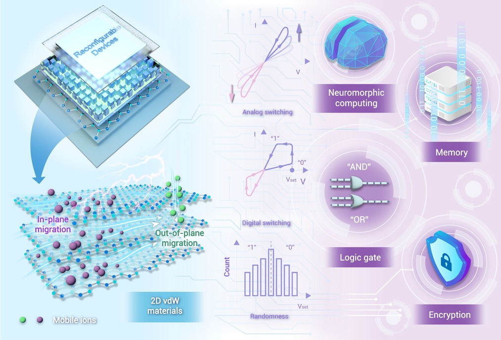
Figure 1.
Schematic diagram of ion migration within 2D vdW materials-based devices, diverse electrical characteristics of these devices, and their applications for information processing
-
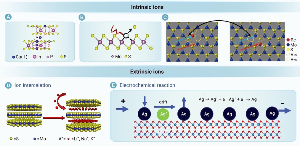
Figure 2.
Schematic representation of the categories of mobile ions in 2D materials
-
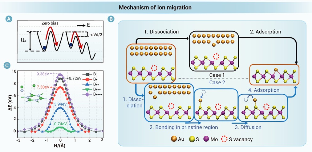
Figure 3.
Schematic representation of the ion migration mechanism in 2D materials
-
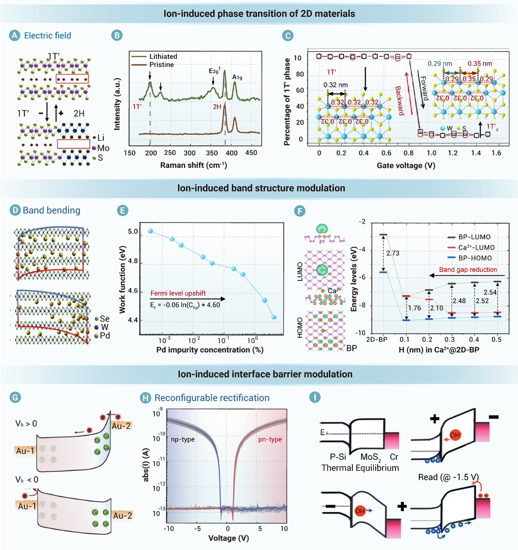
Figure 4.
Modulation of the physical properties of 2D materials through nanoionics
-
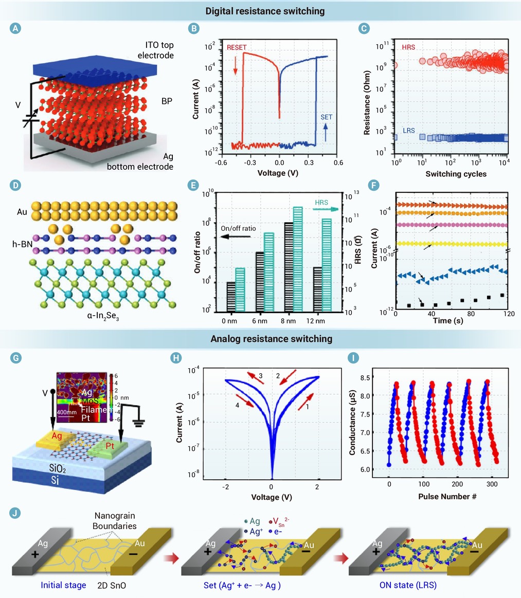
Figure 5.
Ion-driven reconfigurable resistance modulation in a two-terminal device based on 2D materials
-
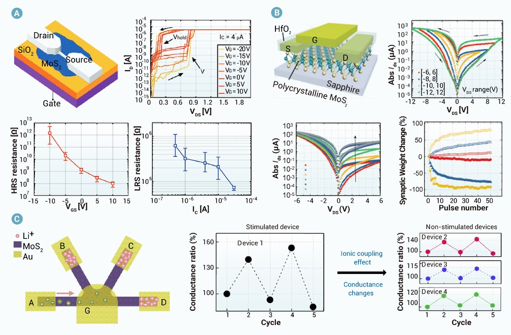
Figure 6.
Ion-driven resistance modulation in a multi-terminal structure based on 2D materials
-
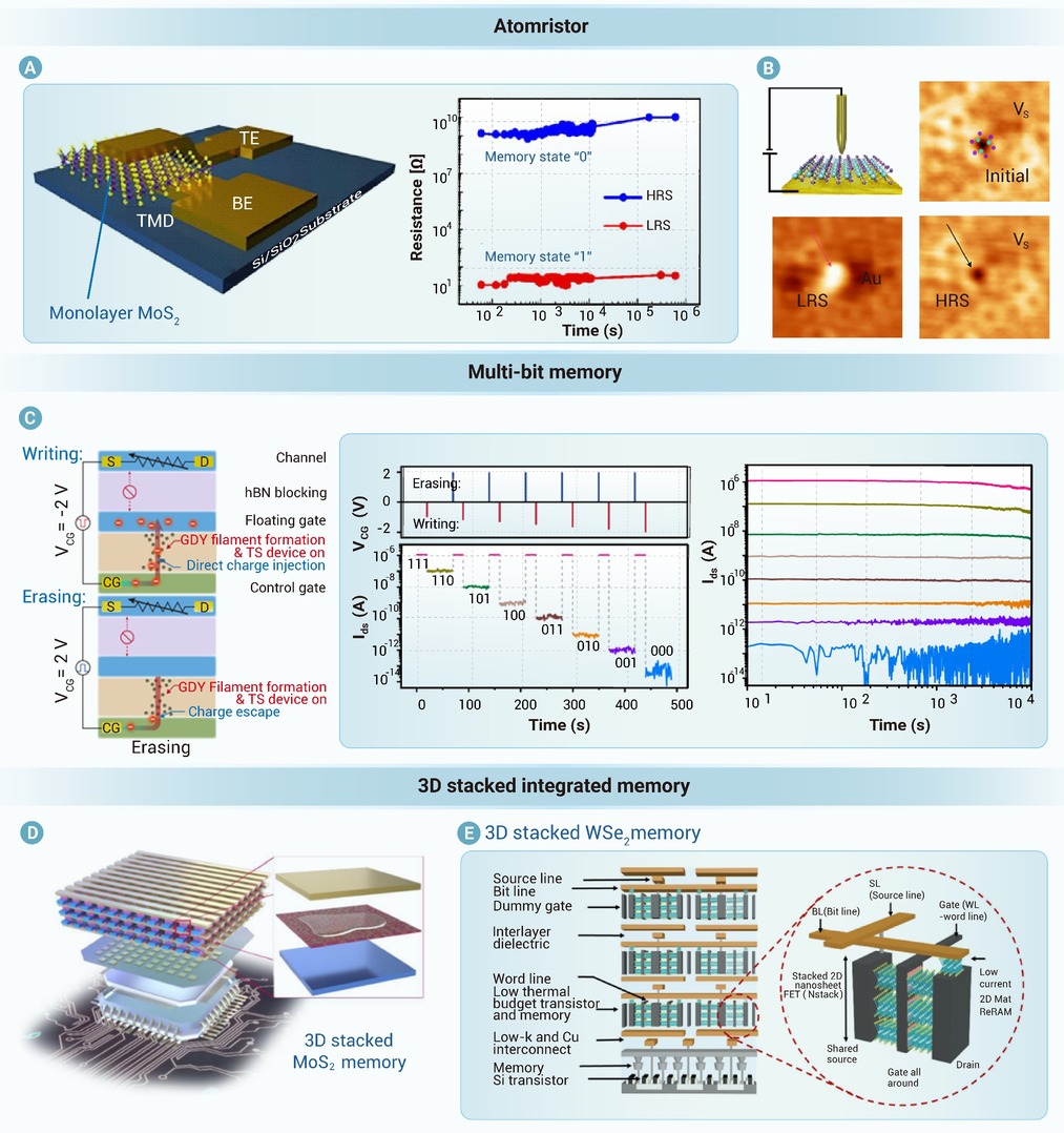
Figure 7.
Memory based on reconfigurable resistance modulation
-
Figure 8.
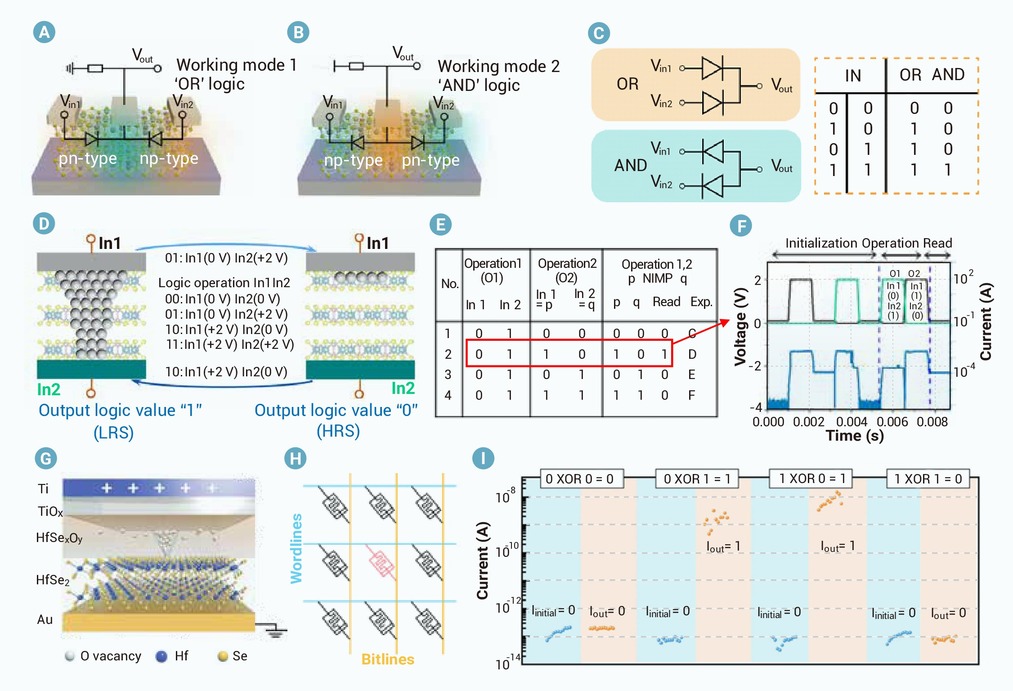
Logic-in-memory based on reconfigurable resistance modulation
-
Figure 9.
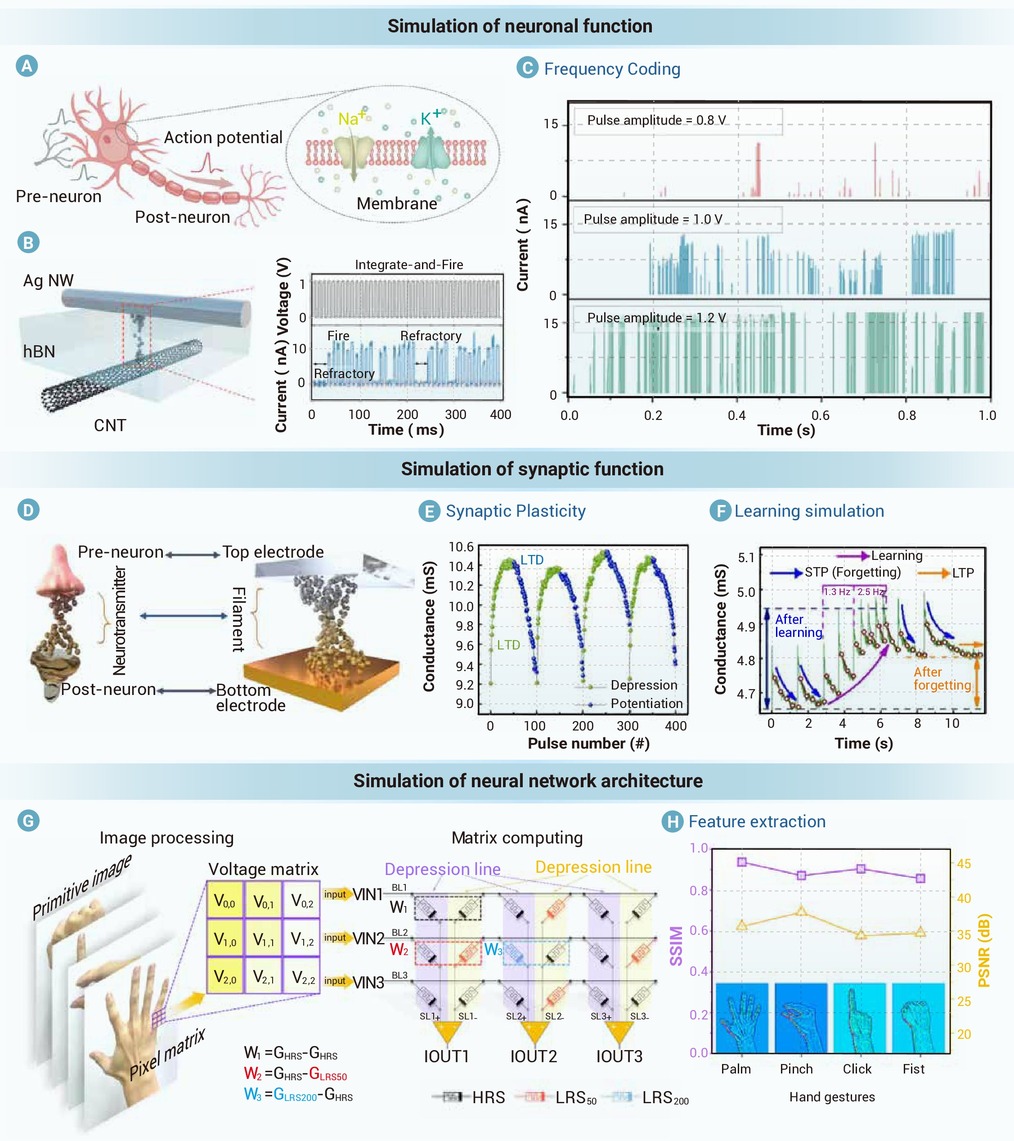
Neuromorphic computing based on reconfigurable resistance modulation
-
Figure 10.
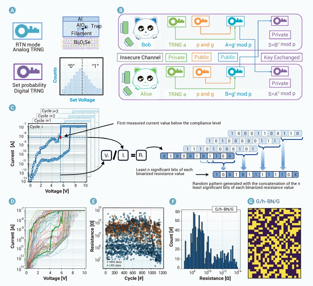
Data encryption based on reconfigurable resistance modulation
-
Figure 11.
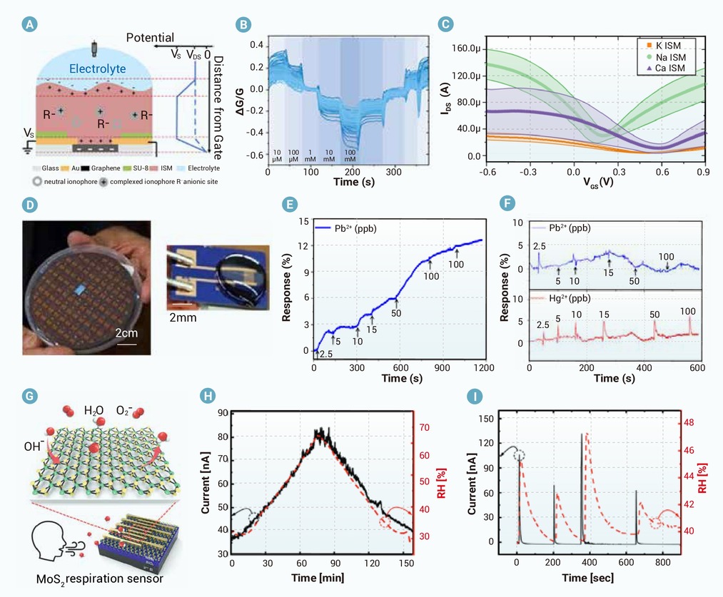
Sensors based on reconfigurable resistance modulation
-
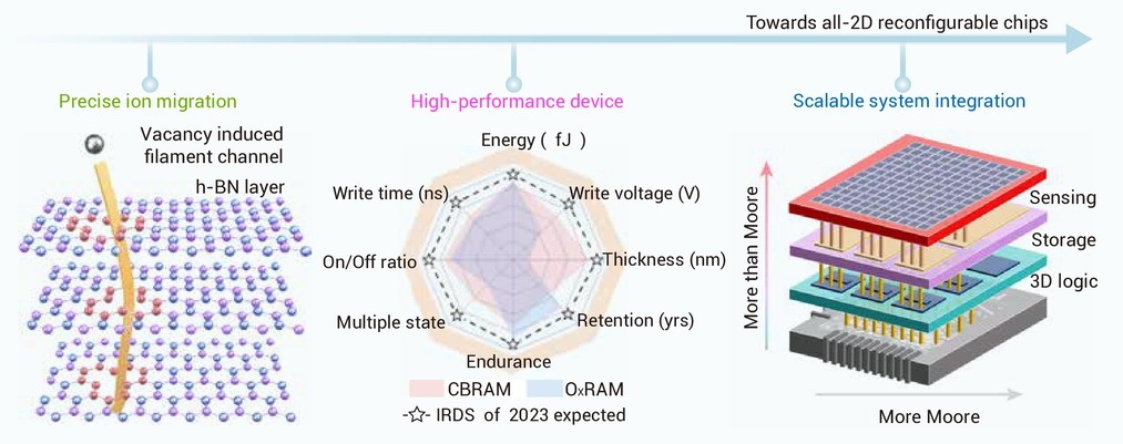
Figure 12.
The schematic illustration of perspectives and challenges for ion-driven 2D materials-based devices, including precise ion migration, high device performance, and scalable system integration. Adapted with permission.143 Copyright 2025, Elsevier. Adapted with permission.308 Copyright 2024, Springer Nature.
