
General photogating: An emerging paradigm for low-dimensional photodetectors
-
GRAPHICAL ABSTRACT
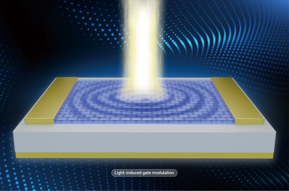
 DownLoad:
Full size image
DownLoad:
Full size image
-
PUBLIC SUMMARY
-
This Review introduces the General Photogating Effect (GPE) for low-dimensional photodetectors.
The GPE unifies light-induced gate modulation across diverse materials and device structures.
Design guidelines for high-performance and multifunctional GPE-based photodetectors are outlined.
-
-
ABSTRACT
Low-dimensional materials have attracted tremendous attention as promising building blocks for novel photodetector construction, providing a versatile platform to explore intriguing photocurrent generation mechanisms. Among them, photogating has been extensively studied and demonstrated to play a pivotal role in low-dimensional photodetectors. Photogating refers to the formation of electric fields induced by localized photocarriers due to trap states or artificial heterostructures, which modulate the material conductance in a gate-like manner. However, with the rapid development of low-dimensional photodetectors, the strategies for realizing light-induced gate modulation have become increasingly diverse, rendering the conventional photogating framework insufficient to encompass emerging device operation mechanisms. To broaden the conceptual scope of photogating, this review revisits its literal meaning, light-induced gate modulation, and uses the concept of General Photogating Effect (GPE) as a framework for integrating and extending related phenomena. First, the underlying generation mechanisms of GPE are summarized, followed by an analysis of the performance characteristics and device architectures of GPE-based photodetectors. Subsequently, representative recent advances are reviewed. Furthermore, the potential of GPE in enhancing overall performance and enabling functional photodetection is discussed. This review aims to refine the framework of photogating, promote a unified understanding of its diverse manifestations, and inspire the design of next-generation low-dimensional photodetectors.-
Keywords:
- Photodetection /
- Heterostructure /
- Low-dimensional Material /
- Photogating /
- Review
-

-
REFERENCES
[1] Koppens F. H., Mueller T., Avouris P., et al. (2014). Photodetectors based on graphene, other two-dimensional materials and hybrid systems. Nat. Nanotech. 9:780−793. DOI:10.1038/nnano.2014.215 [2] Buscema M., Island J. O., Groenendijk D. J., et al. (2015). Photocurrent generation with two-dimensional van der Waals semiconductors. Chem. Soc. Rev. 44:3691−3718. DOI:10.1039/c5cs00106d [3] Long M., Wang P., Fang H., et al. (2018). Progress, challenges, and opportunities for 2D material based photodetectors. Adv. Funct. Mater. 29:1803807. DOI:10.1002/adfm.201803807 [4] Chen Y., Wang Y., Wang Z., et al. (2021). Unipolar barrier photodetectors based on van der Waals heterostructures. Nat. Electron. 4:357−363. DOI:10.1038/s41928-021-00586-w [5] Fu J., Guo Z., Nie C., et al. (2024). Schottky infrared detectors with optically tunable barriers beyond the internal photoemission limit. The Innovation 5:100600. DOI:10.1016/j.xinn.2024.100600 [6] Scales C. and Berini P. (2010). Thin-film Schottky barrier photodetector models. IEEE J. Quantum Electron. 46:633−643. DOI:10.1109/jqe.2010.2046720 [7] Peng Y., Liu J., Fu J., et al. (2025). Emerging thermal detectors based on low-dimensional materials: Strategies and progress. Nanomaterials 15:459. DOI:10.3390/nano15060459 [8] Gabor N. M., Song J. C. W., Ma Q., et al. (2011). Hot carrier-assisted intrinsic photoresponse in graphene. Science 334:648−652. DOI:10.1126/science.1211384 [9] Dai W., Liu W., Yang J., et al. (2020). Giant photothermoelectric effect in silicon nanoribbon photodetectors. Light Sci. Appl. 9:120. DOI:10.1038/s41377-020-00364-x [10] Wei J., Li Y., Wang L., et al. (2020). Zero-bias mid-infrared graphene photodetectors with bulk photoresponse and calibration-free polarization detection. Nat. Commun. 11:6404. DOI:10.1038/s41467-020-20115-1 [11] Ji Z., Liu W., Krylyuk S., et al. (2020). Photocurrent detection of the orbital angular momentum of light. Science 368:763−767. DOI:10.1126/science.aba9192 [12] de Juan F., Grushin A. G., Morimoto T., et al. (2017). Quantized circular photogalvanic effect in Weyl semimetals. Nat. Commun. 8:15995. DOI:10.1038/ncomms15995 [13] Dhara S., Mele E. J. and Agarwal R. (2015). Voltage-tunable circular photogalvanic effect in silicon nanowires. Science 349:726−729. DOI:10.1126/science.aac6275 [14] Fu J., Nie C., Sun F., et al. Photodetectors based on graphene–semiconductor hybrid structures: recent progress and future outlook. Adv. Devices Instrumen. 4:0031. DOI:10.34133/adi.0031 [15] Fang H. and Hu W. (2017). Photogating in low dimensional photodetectors. Adv. Sci. 4:1700323. DOI:10.1002/advs.201700323 [16] Shin J. and Yoo H. (2023). Photogating effect-driven photodetectors and their emerging applications. Nanomaterials 13:882. DOI:10.3390/nano13050882 [17] Liu H., Yi Z. and Chen C. (2025). Advances in photodetectors via photogating effect. Mater. Res. Bull. 192:113628. DOI:10.1016/j.materresbull.2025.113628 [18] Zheng L., Zhou W., Ning Z., et al. (2018). Ambipolar graphene-quantum dot phototransistors with CMOS compatibility. Adv. Opt. Mater. 6:1800985. DOI:10.1002/adom.201800985 [19] Han J., Wang J., Yang M., et al. (2018). Graphene/organic semiconductor heterojunction phototransistors with broadband and bi-directional photoresponse. Adv. Mater. 30:e1804020. DOI:10.1002/adma.201804020 [20] Tu L., Cao R., Wang X., et al. (2020). Ultrasensitive negative capacitance phototransistors. Nat. Commun. 11:101. DOI:10.1038/s41467-019-13769-z [21] Konstantatos G., Badioli M., Gaudreau L., et al. (2012). Hybrid graphene-quantum dot phototransistors with ultrahigh gain. Nat. Nanotechnol. 7:363−368. DOI:10.1038/nnano.2012.60 [22] Ni Z., Ma L., Du S., et al. (2017). Plasmonic silicon quantum dots enabled high-sensitivity ultrabroadband photodetection of graphene-based hybrid phototransistors. ACS Nano 11:9854−9862. DOI:10.1021/acsnano.7b03569 [23] Liu M., Wei J., Qi L., et al. (2024). Photogating-assisted tunneling boosts the responsivity and speed of heterogeneous WSe2/Ta2NiSe5 photodetectors. Nat. Commun. 15:141. DOI:10.1038/s41467-023-44482-7 [24] Han J., Tuo T., Deng W., et al. (2025). 2D/organic photovoltage field-effect transistors. Laser Photonics Rev. 19:2500268. DOI:10.1002/lpor.202500268 [25] Soci C., Zhang A., Xiang B., et al. (2007). ZnO nanowire UV photodetectors with high internal gain. Nano Lett. 7:1003−1009. DOI:10.1021/nl070111x [26] Roy K., Padmanabhan M., Goswami S., et al. (2013). Graphene-MoS2 hybrid structures for multifunctional photoresponsive memory devices. Nat. Nanotechnol. 8:826−830. DOI:10.1038/nnano.2013.206 [27] Lopez-Sanchez O., Lembke D., Kayci M., et al. (2013). Ultrasensitive photodetectors based on monolayer MoS2. Nat. Nanotechnol. 8:497−501. DOI:10.1038/nnano.2013.100 [28] Zhang W., Huang J.-K., Chen C.-H., et al. (2013). High-gain phototransistors based on a CVD MoS2 monolayer. Adv. Mater. 25:3456−3461. DOI:10.1002/adma.201301244 [29] Li Y., Chen G., Zhao S., et al. (2022). Addressing gain-bandwidth trade-off by a monolithically integrated photovoltaic transistor. Sci. Adv. 8:eabq0187. DOI:10.1126/sciadv.abq0187 [30] Pak S., Cho Y., Hong J., et al. (2018). Consecutive junction-induced efficient charge separation mechanisms for high-performance MoS2/quantum dot phototransistors. ACS Appl. Mater. Interfaces 10:38264−38271. DOI:10.1021/acsami.8b14408 [31] Guo N., Xiao L., Gong F., et al. (2020). Light-driven WSe2-ZnO junction field-effect transistors for high-performance photodetection. Adv. Sci. 7:1901637. DOI:10.1002/advs.201901637 [32] Tuo T., Wei L., Han J., et al. (2025). Light-driven Ta2NiSe5/MoSe2 van der Waals heterostructure field-effect Phototransistors. Infrared Phys. Techn. 150:106057. DOI:10.1016/j.infrared.2025.106057 [33] Sassi U., Parret R., Nanot S., et al. (2017). Graphene-based mid-infrared room-temperature pyroelectric bolometers with ultrahigh temperature coefficient of resistance. Nat. Commun. 8:14311. DOI:10.1038/ncomms14311 [34] Gopalan K. K., Janner D., Nanot S., et al. (2017). Mid-infrared pyroresistive graphene detector on LiNbO3. Adv. Opt. Mater. 5:1600723. DOI:10.1002/adom.201600723 [35] Peng Y., Yang Q., Fu J., et al. (2025). Uncooled graphene infrared detectors enabled by pyroelectric photogating for human radiation perception. Laser Photonics Rev. 19:2500218. DOI:10.1002/lpor.202500218 [36] Adinolfi V. and Sargent E. H. (2017). Photovoltage field-effect transistors. Nature 542:324−327. DOI:10.1038/nature21050 [37] Fu J., Jiang H., Nie C., et al. (2023). Polarity-tunable field effect phototransistors. Nano Lett. 23:4923−4930. DOI:10.1021/acs.nanolett.3c00728 [38] Guo X., Wang W., Nan H., et al. (2016). High-performance graphene photodetector using interfacial gating. Optica 3:1066−1070. DOI:10.1364/optica.3.001066 [39] Zhang Z., Wang S., Liu C., et al. (2022). All-in-one two-dimensional retinomorphic hardware device for motion detection and recognition. Nat. Nanotechnol. 17:27−32. DOI:10.1038/s41565-021-01003-1 [40] Deng J., Zong L., Zhu M., et al. (2019). MoS2/HfO2/Silicon‐On‐Insulator dual‐photogating transistor with ambipolar photoresponsivity for high‐resolution light wavelength detection. Adv. Funct. Mater. 29:1906242. DOI:10.1002/adfm.201906242 [41] Wu G., Zhang X., Feng G., et al. (2023). Ferroelectric-defined reconfigurable homojunctions for in-memory sensing and computing. Nat. Mater. 22:1499−1506. DOI:10.1038/s41563-023-01676-0 [42] Jang H., Liu C., Hinton H., et al. (2020). An atomically thin optoelectronic machine vision processor. Adv. Mater. 32:2002431. DOI:10.1002/adma.202002431 [43] Furchi M. M., Polyushkin D. K., Pospischil A., et al. (2014). Mechanisms of photoconductivity in atomically thin MoS2. Nano Lett. 14:6165−6170. DOI:10.1021/nl502339q [44] Chen J., Zhou Z., Kim B. J., et al. (2023). Optoelectronic graded neurons for bioinspired in-sensor motion perception. Nat. Nanotechnol. 18:882−888. DOI:10.1038/s41565-023-01379-2 [45] Xu H., Xu Z., Ren Q., et al. (2026). Two-dimensional materials for integrated sensing. Nat. Mater. DOI:10.1038/s41563-026-02551-4. [46] Wang C.-Y., Liang S.-J., Wang S., et al. (2020). Gate-tunable van der Waals heterostructure for reconfigurable neural network vision sensor. Sci. Adv. 6. eaba6173,DOI:10.1126/sciadv.aba6173. [47] Choi W., Yoon J. S., Lee W. W., et al. (2025). DPP-DTT nanowire phototransistors for optoelectronic synapses in EMG and ECG signal classification. Small 21:e06440. DOI:10.1002/smll.202506440 [48] Fu J., Ji L., Wu Z., et al. (2024). An all-in-one optoelectronic logic device with self-distinguishable dual-band photoresponse. Device 2:100321. DOI:10.1016/j.device.2024.100321 [49] Wang H., Li Z., Li D., et al. (2021). Junction field‐effect transistors based on PdSe2/MoS2 heterostructures for photodetectors showing high responsivity and detectivity. Adv. Funct. Mater. 31:2106105. DOI:10.1002/adfm.202106105 [50] Fu J., Leng C., Ma R., et al. (2024). Photo-driven fin field-effect transistors. Opto-Electronic Science 3:230046. DOI:10.29026/oes.2024.230046 [51] Wang J., Zang H., Yu M. B., et al. (2009). Enhanced sensitivity of small-size (with 1-μm Gate length) junction-field-effect-transistor-based germanium photodetector using two-step germanium epitaxy by ultrahigh vacuum chemical vapor deposition. IEEE Electron Device Lett. 30:1066−1068. DOI:10.1109/led.2009.2029125 [52] She J., Liu X., Liu H., et al. (2025). Ferroelectric tailorable WS2/graphene phototransistors. Nano Lett. 25:11578−11585. DOI:10.1021/acs.nanolett.5c02241 [53] Tsai T. H., Liang Z. Y., Lin Y. C., et al. (2020). Photogating WS2 photodetectors using embedded WSe2 charge puddles. ACS Nano 14:4559−4566. DOI:10.1021/acsnano.0c00098 [54] Tao L., Li H., Sun M., et al. (2018). Enhanced photoresponse in interfacial gated graphene phototransistor with ultrathin Al2O3 dielectric. IEEE Electron Device Lett. 39:987−990. DOI:10.1109/led.2018.2843804 [55] Wu J., Wen Z., Guo B., et al. (2025). Dielectric-free MoS2/VO2 junction field-effect transistor with sensitive and ultrafast photoresponse for light encrypted communication. Adv. Mater. 37:2503294. DOI:10.1002/adma.202503294 [56] Guo N., Hu W., Liao L., et al. (2014). Anomalous and highly efficient InAs nanowire phototransistors based on majority carrier transport at room temperature. Adv. Mater. 26:8203−8209. DOI:10.1002/adma.201403664 [57] Guo Q., Pospischil A., Bhuiyan M., et al. (2016). Black phosphorus mid-infrared photodetectors with high gain. Nano Lett. 16:4648−4655. DOI:10.1021/acs.nanolett.6b01977 [58] Island J. O., Blanter S. I., Buscema M., et al. (2015). Gate controlled photocurrent generation mechanisms in high-gain In2Se3 phototransistors. Nano Lett. 15:7853−7858. DOI:10.1021/acs.nanolett.5b02523 [59] Fu J., Yang C., Nie C., et al. (2023). Vertical photodetectors based on in-situ aligned single-crystalline PbS nanocuboids sandwiched between graphene electrodes. Adv. Opt. Mater. 11:2300584. DOI:10.1002/adom.202300584 [60] Li C., Wu Z., He M., et al. (2025). Photo-driven all-2D van der Waals metal–semiconductor field-effect transistors for high-performance photodetection. J. Mater. Chem. C 13:10650−10657. DOI:10.1039/D5TC01016K [61] Fu J., Nie C., Sun F., et al. (2022). Photo‐driven semimetal-semiconductor field‐effect transistors. Adv. Opt. Mater. 11. DOI:10.1002/adom.202201983. [62] Adinolfi V., Kramer I. J., Labelle A. J., et al. (2015). Photojunction field-effect transistor based on a colloidal quantum dot absorber channel layer. ACS Nano 9:356−362. DOI:10.1021/nn5053537 [63] Madjar A., Paollela A. and Herczfeld P. R. (1993). Light interaction with GaAs MESFET and its applications—a review (invited paper). Microwave Opt. Technol. Lett. 6:22−27. DOI:10.1002/mop.4650060107 [64] Li X., Wang S., Yang Y., et al. (2024). Photovoltage junction memtransistor for optoelectronic in-memory computing. J. Mater. Chem. C 12:12763−12768. DOI:10.1039/D4TC03015J [65] Shan Y., Yin Z., Zhang Y., et al. (2021). Ultrafast and highly sensitive dual-channel FET photodetector based on a two-dimensional MoS2 homojunction. ACS Appl. Mater. Interfaces 13:54194−54203. DOI:10.1021/acsami.1c16891 [66] Liu X., Zhu J., Shan Y., et al. (2024). An ultrasensitive and broad-spectrum MoS2 photodetector with extrinsic response using surrounding homojunction. Adv. Sci. 11:2408299. DOI:10.1002/advs.202408299 [67] Xiao L., Nie C., Jiang Y., et al. (2024). Ultralow-noise MoS2/Type II superlattice mixed-dimensional van der Waals barrier long-wave infrared detector. ACS Appl. Mater. Interfaces 16:30478−30484. DOI:10.1021/acsami.4c00956 [68] Xiao L., Fu J., Zhu P., et al. (2024). Pixel-integrated Mie metasurface long-wave multispectral type II superlattice detector. Appl. Phys. Lett. 124:091108. DOI:10.1063/5.0185320 [69] Xiao L., Zhu P., Li N., et al. (2022). Gradual funnel photon trapping enhanced InAs/GaSb type-II superlattice infrared detector. Opt. Express 30:38009−38015. DOI:10.1364/OE.468812 [70] Lohstroh J. (1974). The JFET as a photosensitive cell in image sensor arrays. 1974 IEEE International Solid-State Circuits Conference. Digest of Technical Papers. [71] Shannon J. M. and Lohstroh J. (1974). JFET optical detectors in the charge storage mode. IEEE T. Electron Dev. 21:720−728. DOI:10.1109/T-ED.1974.17999 [72] Shu X., Wu J., Zhong F., et al. (2024). High-responsivity, high-detectivity, broadband infrared photodetector based on MoS2/BP/MoS2 junction field-effect transistor. Appl. Phys. Lett. 124:181101. DOI:10.1063/5.0205803 [73] Guan H., Hong J., Wang X., et al. (2021). Broadband, high-sensitivity graphene photodetector based on ferroelectric polarization of lithium niobate. Adv. Opt. Mater. 9:2100245. DOI:10.1002/adom.202100245 [74] Fukushima S., Shimatani M. and Ogawa S. (2023). Graphene infrared photodetectors using type-II InAs/InGaSb superlattices. Infrared Technology and Applications XLIX. SPIE. [75] Liu W., Lv J., Peng L., et al. (2022). Graphene charge-injection photodetectors. Nat. Electron. 5:281−288. DOI:10.1038/s41928-022-00755-5 [76] Deng J., Shao J., Lu B., et al. (2018). Interface coupled photodetector (ICPD) with high photoresponsivity based on Silicon-on-Insulator substrate (SOI). IEEE J. Electron Dev. 6:557−564. DOI:10.1109/jeds.2017.2788403 [77] Liao F., Deng J., Chen X., et al. (2020). A dual-gate MoS2 photodetector based on interface coupling effect. Small 16:1904369. DOI:10.1002/smll.201904369 [78] Pang Y., Zhou Y., Tong L., et al. (2024). 2D dual gate field-effect transistor enabled versatile functions. Small 20:2304173. DOI:10.1002/smll.202304173 [79] Deng J., Guo Z., Zhang Y., et al. (2019). MoS2/Silicon-on-Insulator heterojunction field-effect-transistor for high-performance photodetection. IEEE Electron Device Lett. 40:423−426. DOI:10.1109/LED.2019.2892782 [80] Li L., Li S., Wang W., et al. (2024). Adaptative machine vision with microsecond-level accurate perception beyond human retina. Nat. Commun. 15:6261. DOI:10.1038/s41467-024-50488-6 [81] Xiong J., Yu Q., Hou X., et al. (2024). Short-wave infrared photodetectors based on β-In2Se3/Te heterojunctions for optical communication and polarimetric imaging applications. Adv. Funct. Mater. 34:2314972. DOI:10.1002/adfm.202314972 [82] Huang Z., Wang W., Wang S., et al. (2024). Gate-tunable positive and negative photoresponses based on a mixed-dimensional Ga2O3/WSe2 junction field-effect transistor for logic operation. Photonics Res. 12:2804−2811. DOI:10.1364/PRJ.534338 [83] Zhou Y., Li F., Li W., et al. (2024). MoS2/GaN junction field-effect transistors with ultralow subthreshold swing and high on/off ratio via thickness engineering for logic inverters. Adv. Funct. Mater. 34:2410954. DOI:10.1002/adfm.202410954 [84] Sze S. and Ng K. K. (2006). Physics of semiconductor devices: third edition. Physics of Semiconductor Devices: Third Edition:1-815. DOI:10.1002/9780470068328. [85] Wang F., Zhang T., Xie R., et al. (2023). How to characterize figures of merit of two-dimensional photodetectors. Nat. Commun. 14:2224. DOI:10.1038/s41467-023-37635-1 [86] Bielecki Z., Achtenberg K., Kopytko M., et al. (2022). Review of photodetectors characterization methods. Bulletin of the Polish Academy of Sciences-Technical Sciences B Pol. Acad. Sci-Tech. 70. e140534,DOI:10.24425/bpasts.2022.140534. [87] Hu C., Dong D., Yang X., et al. (2017). Synergistic effect of hybrid PbS quantum dots/2D-WSe2 toward high performance and broadband phototransistors. Adv. Funct. Mater. 27:1603605. DOI:10.1002/adfm.201603605 [88] Luo P., Zhuge F., Wang F., et al. (2019). PbSe quantum dots sensitized high-mobility Bi2O2Se nanosheets for high-performance and broadband photodetection beyond 2 μm. ACS Nano 13:9028−9037. DOI:10.1021/acsnano.9b03124 [89] Zheng D., Fang H., Wang P., et al. (2016). High-performance ferroelectric polymer side-gated CdS nanowire ultraviolet photodetectors. Adv. Funct. Mater. 26:7690−7696. DOI:10.1002/adfm.201603152 [90] Huang H., Wang J., Hu W., et al. (2016). Highly sensitive visible to infrared MoTe2 photodetectors enhanced by the photogating effect. Nanotechnology 27:445201. DOI:10.1088/0957-4484/27/44/445201 [91] Kind H., Yan H. Q., Messer B., et al. (2002). Nanowire ultraviolet photodetectors and optical switches. Adv. Mater. 14:158−160. DOI:3.0.Co;2-w">10.1002/1521-4095(20020116)14:2<158::Aid-adma158>3.0.Co;2-w [92] Vashishtha P., Abidi I. H., Giridhar S. P., et al. (2024). CVD-grown monolayer MoS2 and GaN thin film heterostructure for a self-powered and bidirectional photodetector with an extended active spectrum. ACS Appl. Mater. Interfaces 16:31294−31303. DOI:10.1021/acsami.4c03902 [93] Nikitskiy I., Goossens S., Kufer D., et al. (2016). Integrating an electrically active colloidal quantum dot photodiode with a graphene phototransistor. Nat. Commun. 7:11954. DOI:10.1038/ncomms11954 [94] Chow P. C. Y., Matsuhisa N., Zalar P., et al. (2018). Dual-gate organic phototransistor with high-gain and linear photoresponse. Nat. Commun. 9:4546. DOI:10.1038/s41467-018-06907-6 [95] Wang L., Wang H., Liu J., et al. (2024). Negative photoconductivity transistors for visuomorphic computing. Adv. Mater. 36:2403538. DOI:10.1002/adma.202403538 [96] Jariwala D., Marks T. J. and Hersam M. C. (2017). Mixed-dimensional van der Waals heterostructures. Nat. Mater. 16:170−181. DOI:10.1038/nmat4703 [97] Liu Y., Weiss N. O., Duan X., et al. (2016). Van der Waals heterostructures and devices. Nat. Rev. Mater. 1:16042. DOI:10.1038/natrevmats.2016.42 [98] Kufer D., Nikitskiy I., Lasanta T., et al. (2015). Hybrid 2D-0D MoS2-PbS quantum dot photodetectors. Adv. Mater. 27:176−180. DOI:10.1002/adma.201402471 [99] Choi W., Cho M. Y., Konar A., et al. (2012). High-detectivity multilayer MoS2 phototransistors with spectral response from ultraviolet to infrared. Adv. Mater. 24:5832−5836. DOI:10.1002/adma.201201909 [100] Kufer D. and Konstantatos G. (2015). Highly sensitive, encapsulated MoS2 photodetector with gate controllable gain and speed. Nano Lett. 15:7307−7313. DOI:10.1021/acs.nanolett.5b02559 [101] Fu J., Nie C., Sun F., et al. (2024). Bionic visual-audio photodetectors with in-sensor perception and preprocessing. Sci. Adv. 10:eadk8199. DOI:10.1126/sciadv.adk8199 [102] Han C., Liu X., Han X., et al. (2022). High-performance phototransistor based on graphene/organic heterostructure for in-chip visual processing and pulse monitoring. Adv. Funct. Mater. 32:2209680. DOI:10.1002/adfm.202209680 [103] Pi L., Wang P., Liang S.-J., et al. (2022). Broadband convolutional processing using band-alignment-tunable heterostructures. Nat. Electron. 5:248−254. DOI:10.1038/s41928-022-00747-5 [104] Luo W., Weng Q., Long M., et al. (2018). Room-temperature single-photon detector based on single nanowire. Nano Lett. 18:5439−5445. DOI:10.1021/acs.nanolett.8b01795 [105] Zheng D., Wang J., Hu W., et al. (2016). When nanowires meet ultrahigh ferroelectric field-high-performance full-depleted nanowire photodetectors. Nano Lett. 16:2548−2555. DOI:10.1021/acs.nanolett.6b00104 [106] Zhang K., Peng M., Yu A., et al. (2019). A substrate-enhanced MoS2 photodetector through a dual-photogating effect. Mater. Horiz. 6:826−833. DOI:10.1039/c8mh01429a [107] Fu J., Que L., Jiang H., et al. (2020). Effects of doping graphene on the performance of graphene-silicon hybrid photoconductive detectors. Nanotechnology 31:485201. DOI:10.1088/1361-6528/abb108 [108] Hao J., Changbin N., Jintao F., et al. (2020). Ultrasensitive and fast photoresponse in graphene/silicon-on-insulator hybrid structure by manipulating the photogating effect. Nanophotonics 9:3663−3672. DOI:10.1515/nanoph-2020-0261 [109] Jiang H., Wang M., Fu J., et al. (2022). Ultrahigh photogain short-wave infrared detectors enabled by integrating graphene and hyperdoped silicon. ACS Nano 16:12777−12785. DOI:10.1021/acsnano.2c04704 [110] Lee I., Kang W. T., Kim J. E., et al. (2020). Photoinduced tuning of Schottky barrier height in graphene/MoS2 heterojunction for ultrahigh performance short channel phototransistor. ACS Nano 14:7574−7580. DOI:10.1021/acsnano.0c03425 [111] De Fazio D., Uzlu B., Torre I., et al. (2020). Graphene-quantum dot hybrid photodetectors with low dark-current readout. ACS Nano 14:11897−11905. DOI:10.1021/acsnano.0c04848 [112] Joy R. C. and Linvill J. G. (1968). Phototransistor operation in the charge storage mode. IEEE T. Electron Dev. 15:237−248. DOI:10.1109/T-ED.1968.16172 [113] Liang F.-X., Jiang J.-J., Zhao Y.-Z., et al. (2020). Fabrication of MAPbBr3 single crystal p-n photodiode and n-p-n phototriode for sensitive light detection application. Adv. Funct. Mater. 30:2001033. DOI:10.1002/adfm.202001033 [114] Li H., Ye L. and Xu J. (2017). High-performance broadband floating-base bipolar phototransistor based on WSe2/BP/MoS2 heterostructure. ACS Photonics 4:823−829. DOI:10.1021/acsphotonics.6b00778 [115] Zhou W., Zheng L., Ning Z., et al. (2021). Silicon: Quantum dot photovoltage triodes. Nat Commun 12:6696. DOI:10.1038/s41467-021-27050-9 [116] Sahni S., Luo X., Liu J., et al. (2008). Junction field-effect-transistor-based germanium photodetector on silicon-on-insulator. Opt. Lett. 33:1138−1140. DOI:10.1364/ol.33.001138 [117] Edwards W. D. (1980). Two and three terminal gallium arsenide FET optical detectors. IEEE Electron Device Lett. 1:149−150. DOI:10.1109/EDL.1980.25268 [118] Macdonald R. I. (1981). High-gain optical-detection with GaAs field-effect transistors. Appl. Opt. 20:591−594. DOI:10.1364/ao.20.000591 [119] Chen C. Y., Cho A. Y., Bethea C. G., et al. (1983). Ultrahigh speed modulation-doped heterostructure field-effect photodetectors. Appl. Phys. Lett. 42:1040−1042. DOI:10.1063/1.93835 [120] Nair R. R., Blake P., Grigorenko A. N., et al. (2008). Fine structure constant defines visual transparency of graphene. Science 320:1308−1308. DOI:10.1126/science.1156965 [121] Lee H. S., Baik S. S., Lee K., et al. (2015). Metal semiconductor field-effect transistor with MoS2/conducting NiOx van der Waals Schottky interface for intrinsic high mobility and photoswitching speed. ACS Nano 9:8312−8320. DOI:10.1021/acsnano.5b02785 [122] Ye Y., Dai L., Wen X., et al. (2010). High-performance single CdS nanobelt metal-semiconductor field-effect transistor-based photodetectors. ACS Appl. Mater. Interfaces 2:2724−2727. DOI:10.1021/am100661x [123] Wang B., Zhang N., You J., et al. (2025). Visible–near-infrared wavelength-selective photodetection and imaging based on floating-gate phototransistors. InfoMat 7:e12661. DOI:10.1002/inf2.12661 [124] Prajapat P., Vashishtha P. and Gupta G. (2025). High-temperature resilient neuromorphic device based on optically configured monolayer MoS2 for cognitive computing. Small 21:2411596. DOI:10.1002/smll.202411596 [125] Jiang H., Wei J., Sun F., et al. (2022). Enhanced photogating effect in graphene photodetectors via potential fluctuation engineering. ACS Nano 16:4458−4466. DOI:10.1021/acsnano.1c10795 [126] He J., Chen K., Huang C., et al. (2020). Explicit gain equations for single crystalline photoconductors. ACS Nano 14:3405−3413. DOI:10.1021/acsnano.9b09406 [127] Goossens S., Navickaite G., Monasterio C., et al. (2017). Broadband image sensor array based on graphene–CMOS integration. Nat. Photonics 11:366−371. DOI:10.1038/nphoton.2017.75 [128] Yang H., Heo J., Park S., et al. (2012). Graphene barristor, a triode device with a gate-controlled Schottky barrier. Science 336:1140−1143. DOI:10.1126/science.1220527 [129] Kufer D. and Konstantatos G. (2016). Photo-FETs: phototransistors enabled by 2D and 0D nanomaterials. ACS Photonics 3:2197−2210. DOI:10.1021/acsphotonics.6b00391 [130] Gao H., Jiang X., Ma X., et al. (2025). Bio-inspired mid-infrared neuromorphic transistors for dynamic trajectory perception using PdSe2/pentacene heterostructure. Nat. Commun. 16:5241. DOI:10.1038/s41467-025-60311-5 [131] Yang Z., Albrow-Owen T., Cai W., et al. (2021). Miniaturization of optical spectrometers. Science 371:eabe0722. DOI:10.1126/science.abe0722 [132] Zhang Y., Yang E., Yoon H. H., et al. (2025). Reconstructive spectrometers: hardware miniaturization and computational reconstruction. eLight 5:23. DOI:10.1186/s43593-025-00101-0 [133] Fu J., Jiang H., Liu X., et al. (2026). Transistor-type optoelectronic sensors from light intensity detection to multifunctional perception. Nat. Sens. 1:209−221. DOI:10.1038/s44460-026-00035-1 [134] Polat E. O., Mercier G., Nikitskiy I., et al. (2019). Flexible graphene photodetectors for wearable fitness monitoring. Sci. Adv. 5:eaaw7846. DOI:10.1126/sciadv.aaw7846 [135] Kim J., Kwon S.-M., Kang Y. K., et al. A skin-like two-dimensionally pixelized full-color quantum dot photodetector. Sci. Adv. 5:eaax8801. DOI:10.1126/sciadv.aax8801. [136] Liu Y., Huang Y. and Duan X. (2019). Van der Waals integration before and beyond two-dimensional materials. Nature 567:323−333. DOI:10.1038/s41586-019-1013-x [137] Lien M.-B., Liu C.-H., Chun I. Y., et al. (2020). Ranging and light field imaging with transparent photodetectors. Nat. Photonics 14:143−148. DOI:10.1038/s41566-019-0567-3 -
ABOUT THIS ARTICLE
Cite this article:
Fu J., Nie C., Sun F., et al. (2026). General photogating: An emerging paradigm for low-dimensional photodetectors. The Innovation Materials 4:100229. https://doi.org/10.59717/j.xinn-mater.2026.100229
Welcome!
To request copyright permission to republish or share portions of our works, please visit Copyright Clearance Center's (CCC) Marketplace website at marketplace.copyright.com.
Export File
Citation
Fu J., Nie C., Sun F., et al. (2026). General photogating: An emerging paradigm for low-dimensional photodetectors. The Innovation Materials 4:100229. https://doi.org/10.59717/j.xinn-mater.2026.100229

Format
Content
-
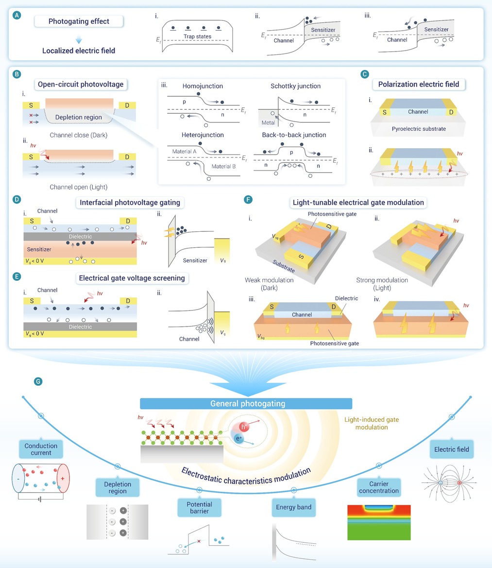
Figure 1.
Illustration of the GPE
-
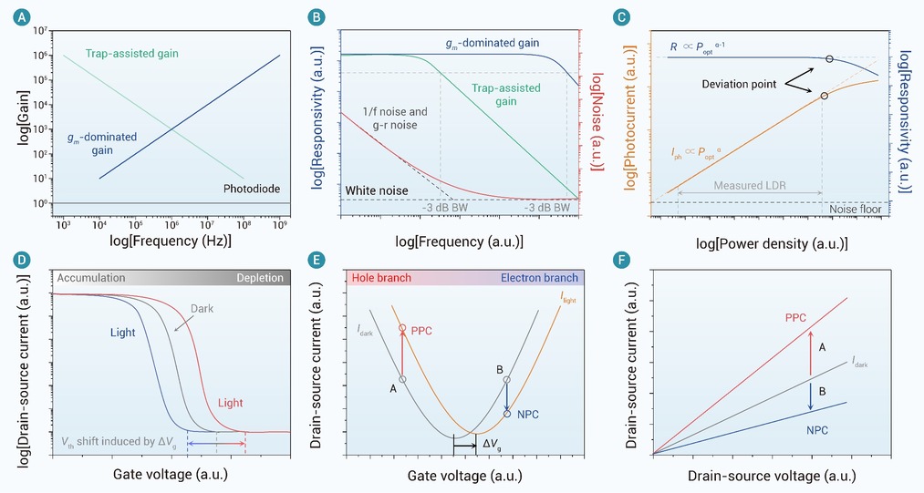
Figure 2.
Characteristics of GPE-based photodetectors
-
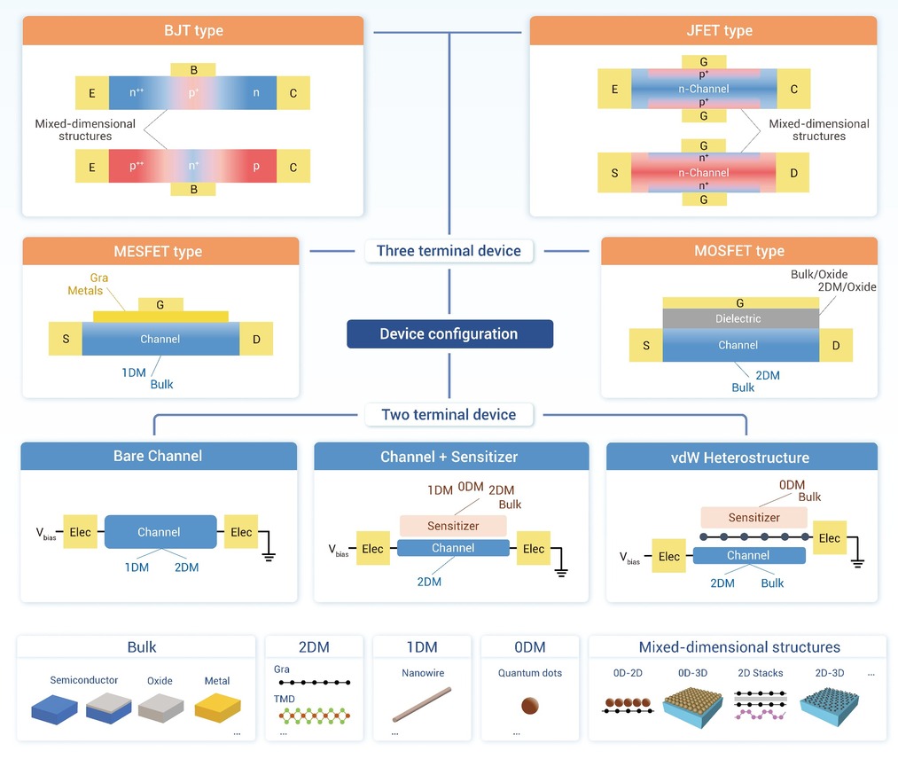
Figure 3.
Main device configurations and material systems of GPE-based photodetectors.
-
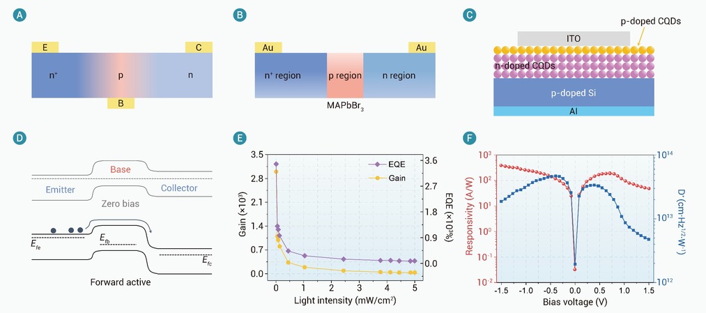
Figure 4.
BJT-type photodetectors with GPE
-
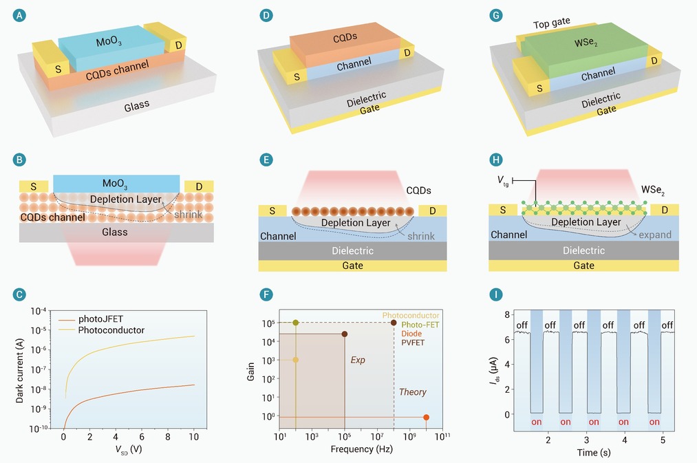
Figure 5.
JFET-type photodetectors with GPE
-
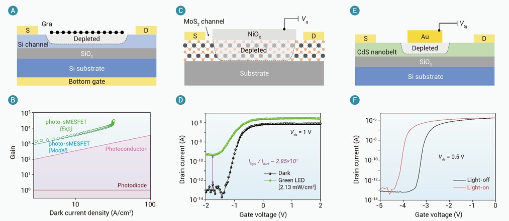
Figure 6.
MESFET-type photodetectors with GPE
-
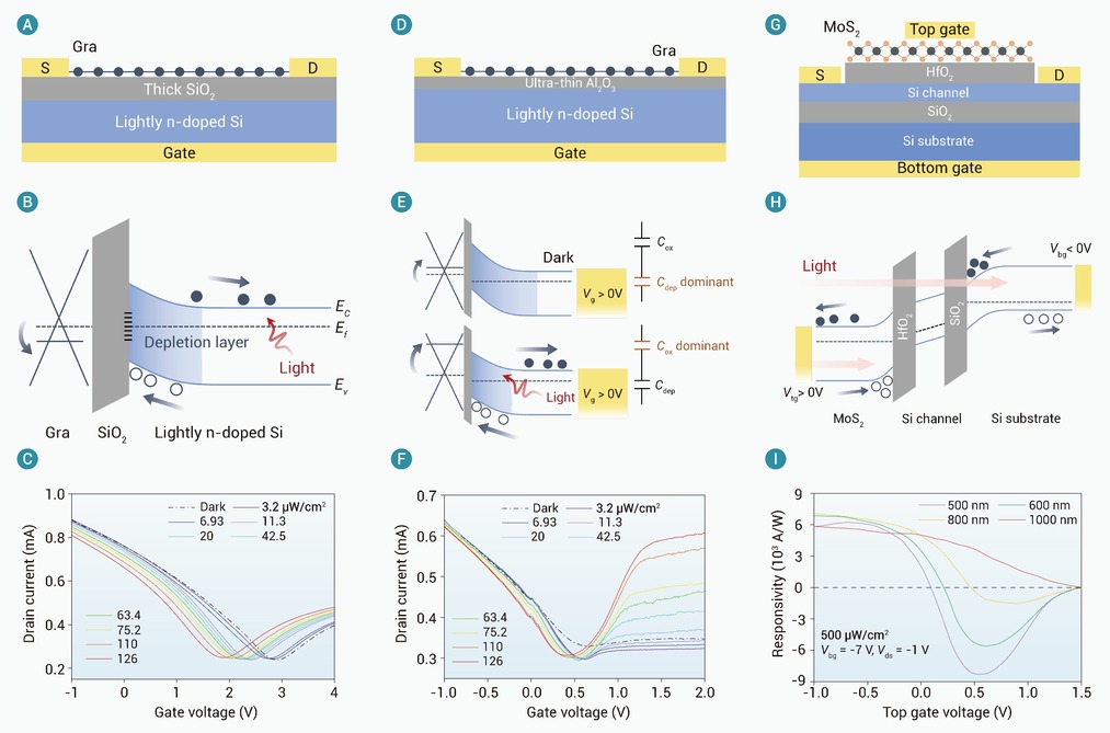
Figure 7.
MOSFET-type photodetectors with GPE
-
Figure 8.
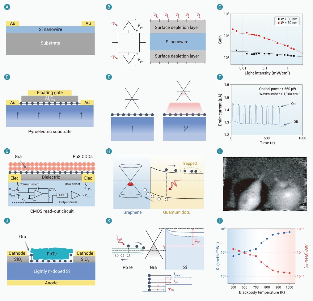
Two-terminal GPE-based devices
-
Figure 9.
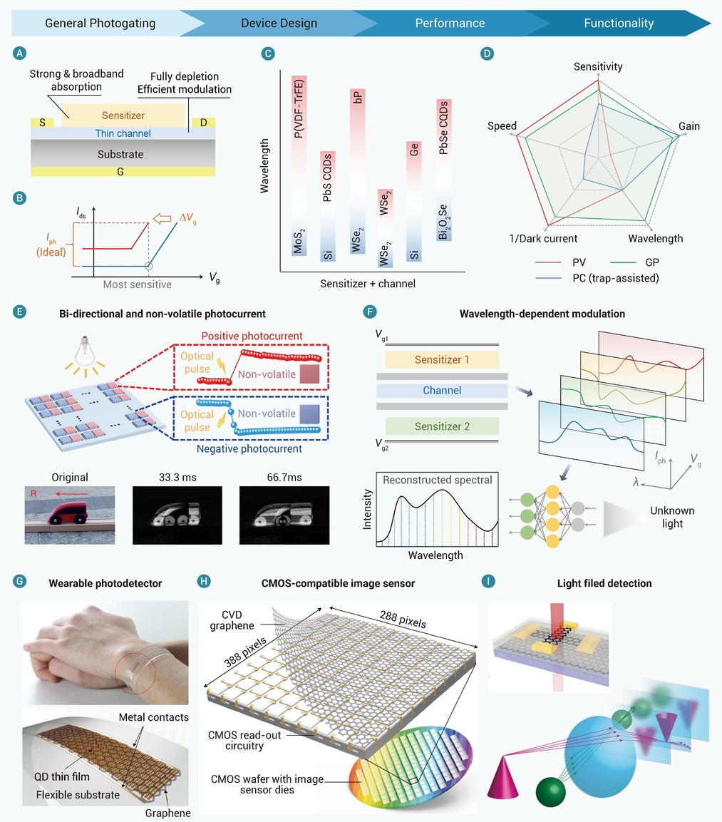
Perspectives for photodetectors with GPE.
